
 Business
> Industrial Devices
> Automation Controls Top
> Components & Devices
> Relays / Couplers
> PhotoMOS
> PhotoMOS Cautions for Use
Business
> Industrial Devices
> Automation Controls Top
> Components & Devices
> Relays / Couplers
> PhotoMOS
> PhotoMOS Cautions for Use
PhotoMOS Cautions for Use

SAFETY WARNINGS
- Do not use the product under conditions that exceed the range of its specifications. It may cause overheating, smoke, or fire.
- Do not touch the recharging unit while the power is on. There is a danger of electrical shock. Be sure to turn off the power when performing mounting, maintenance, or repair operations on the device (including connecting parts such as the terminal board and socket).
- Check the wiring diagrams in the catalog and be sure to connect the terminals correctly. If the device is energized with short circuit or any wrong connection, it may cause unexpected malfunction, abnormal heat or fire.
PhotoMOS Cautions for Use
■Derating design
Derating is a significant factor for reliable design and product life. Even if the conditions of use (temperature, current, voltage, etc.) of the product are within the absolute maximum ratings, reliability may be lowered remarkably when continuously used in high load conditions (high temperature, high humidity, high current, high voltage, etc.) Therefore, please derate sufficiently below the absolute maximum ratings and evaluate the device in the actual condition.
Moreover, regardless of the application, if malfunctioning can be expected to pose high risk to human life or to property, or if products are used in equipment otherwise requiring high operational safety, in addition to designing double circuits, that is, incorporating features such as a protection circuit or a redundant circuit, safety testing should also be carried out.
■Applying stress that exceeds the absolute maximum rating
If the voltage or current value for any of the terminals exceeds the absolute maximum rating, internal elements will deteriorate because of the overvoltage or overcurrent. In extreme cases, wiring may melt, or silicon P/N junctions may be destroyed.
Therefore, the circuit should be designed in such a way that the load never exceed the absolute maximum ratings, even momentarily.
■Input voltage (for Voltage-sensitive type)
For rising and dropping ratio of input voltage (dv/dt), maintain Min. 100 mV/ms.
■Oscillation circuit and control circuit (for CC Type)
The oscillation circuit and control circuit of product may be destroyed by external noise, surge, static electricity and so on.
For noise effect to peripheral circuits when oscillation circuit operates, please implement safety measures on the system before use by verifying operation under the actual design.
■Deterioration and destruction caused by discharge of static electricity
This phenomenon is generally called static electricity destruction, and occurs when static electricity generated by various factors is discharged while the PhotoMOS® terminals are in contact, producing internal destruction of the element.
To prevent problems from static electricity, the following precautions and measures should be taken when using your device.
- 1.Employees handling PhotoMOS® should wear anti-static clothing and should be grounded through protective resistance of 500 kΩ to 1 MΩ.
- 2.A conductive metal sheet should be placed over the worktable. Measuring instruments and jigs should be grounded.
- 3.When using soldering irons, either use irons with low leakage current, or ground the tip of the soldering iron. (Use of low-voltage soldering irons is also recommended.)
- 4.Devices and equipment used in assembly should also be grounded.
- 5.When packing printed circuit boards and equipment, avoid using high-polymer materials such as foam styrene, plastic, and other materials which carry an electrostatic charge.
- 6.When storing or transporting PhotoMOS®, the environment should not be conducive to generating static electricity (for instance, the humidity should be between 45% and 60%), and PhotoMOS® should be protected using conductive packing materials.
■Unused terminals
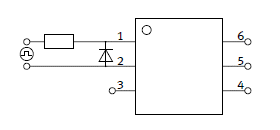
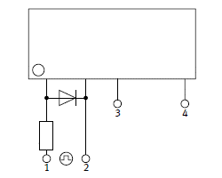
The No. 3 terminal is used with the circuit inside the device. Therefore, do not connect it to the external circuitry with either connection method A, B or C. (1 Form A 6-pin type)
■Short across terminals
Do not short circuit between terminals when device is energized, since there is possibility of breaking of the internal IC.
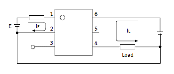
■Surge voltages at the input
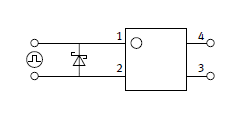
If reverse surge voltages are present at the input terminals, connect a diode in reverse parallel across the input terminals and keep the reverse voltages below the reverse breakdown voltage.
Typical circuits are below shown.
| 1. 6-pin | |
|---|---|
|
| 2. Power type | |
|---|---|
|
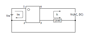
■Reverse voltages at the input (for CC Type)
If reverse voltages are present at the input terminals, for example, connect a schottky barrier diode in reverse parallel across the input terminals and keep the reverse voltages below the reverse breakdown voltage. Typical circuit is shown below.
|
■Recommended LED forward current or recommended input voltage
Design in accordance with the recommended operating conditions for each product.
Since these conditions are affected by the operating environment, ensure conformance with all relevant specifications.
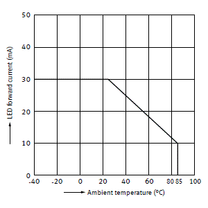
■LED forward current vs. ambient temperature characteristics
Please keep the LED forward current to within the range given below.
(*Please check the reference data in each catalog for products with maximum ambient temperature (oeprating) over 85°C.)
|
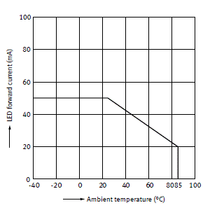
| For AQV209G, APV1111GV, APV3111GV | |
|---|---|
|
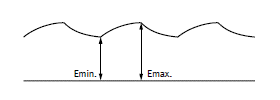
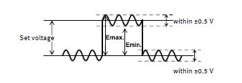
■Ripple in the input power supply
If ripple is present in the input power supply, observe the following:
- 1.For LED forward current at Emin, please maintain the value mentioned at “■ Recommended LED forward current.”
- 2.Please make sure for the LED forward current for Emax. is less than the current value of the “■ Absolute maximum ratings.”
- 3.Please maintain the input voltage at least 4 V for Emin. (GU, RF and Power voltage-sensitive type).
- 4.Please make sure the input voltage for Emax. is no higher than 6 V (GU and RF voltage-sensitive type).
- 5.Please make sure the input voltage for Emax. is no higher than 30 V (Power voltage-sensitive type).
- 6.Please maintain the input voltage at least 3 V for Emin. (for CC Type)
- 7.Please make sure the input voltage for Emax. is no higher than 5.5 V. (for CC Type)
|
- 8.Please keep amplitude voltage of ripple within ±0.5 V. (for CC Type)
|
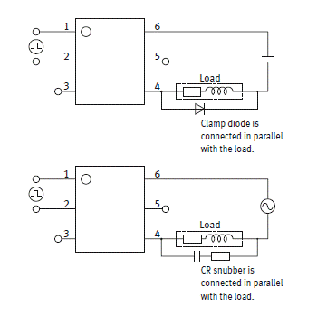
■Output spike voltages
- 1.If an inductive load generates spike voltages which exceed the absolute maximum rating, the spike voltage shall be limited.
Representative circuit examples of AC/DC dual use type are shown below.
There are the same with DC only type.
| 1. 6-pin | |
|---|---|
|
| 2. Power type | |
|---|---|
|
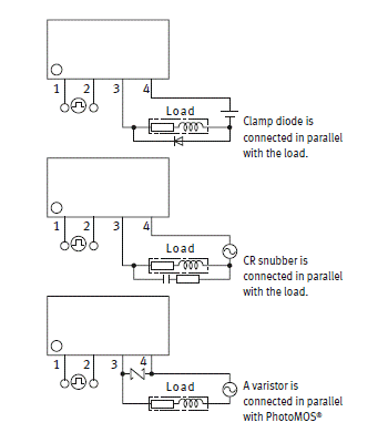
| 3. CC Type | |
|---|---|
|
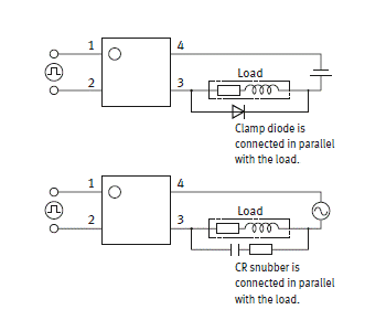
- 2.When Clamp diode or CR Snubber is used in the circuit, the spike voltages from the load are limited. But the longer wire may become the inductance and cause the spike voltage. Keep the wire as short as possible.
■Output Waveform (CC Type)
This product has the capacitor coupled isolation. Therefore, if output waveform fluctuates along the time axis (e.g. AC waveform or pulsating waveform), it may affect the operation of this product and peripheral circuit. Please evaluate the device in the actual condition.
■Continual DC bias (AQV259 and AQV258)
If a continual DC bias will be applied between the input and output, the breakdown voltage of the switching element MOSFET on the output side may degrade. Therefore, be sure to test the product under actual conditions. Example of circuits that will cause degradation of breakdown voltage of MOSFET is given below.
|
■Connections Between Input and Output (CC Type)
If you wish to use the product with a connection between input and output, you may not obtain expected performance. Therefore, please be sure to evaluate the device in the actual usage. A circuit example is shown below that may negatively affect PhotoMOS characteristics.
|
■Cleaning solvents compatibility
Cleaning the solder flux should use the immersion washing with an organic solvent. If you have to use ultrasonic cleaning, please adopt the following conditions and check that there are no problems in the actual usage.
- Frequency: 27 to 29 kHz
- Ultrasonic output: No greater than 0.25 W/cm2 *
- Cleaning time: 30 s or less
- Others: Float PC board and the device in the cleaning solvent to prevent from contacting the ultrasonic vibrator.
* Applies to unit area ultrasonic output for ultrasonic baths
■Notes for mounting
- 1.When different kinds of packages are mounted on PC board, temperature rise at soldering lead is highly dependent on package size. Therefore, please set the lower temperature soldering condition than the conditions of item “■ Soldering”, and confirm the temperature condition of actual usage before soldering.
- 2.When soldering condition exceeds our recommendation, the PhotoMOS® characteristics may be adversely affected. It may occur package crack or bonding wire breaking because of thermal expansion unconformity and resin strength reduction. Please contact us about the propriety of the condition.
- 3.Please confirm the heat stress by using actual board because it may be changed by board condition or manufacturing process condition
- 4.Solder creepage, wettability, or soldering strength will be affected by the soldering condition or used soldering type. Please check them under the actual production condition in detail.
- 5.Please apply coating when the device returns to a room temperature.
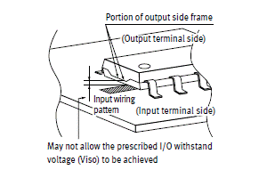
■Input wiring pattern
- 1.With AQY* or AQW* series avoid installing the input (LED side) wiring pattern to the bottom side of the package if you require the specified I/O isolation voltage (Viso) after mounting the PC board. Since part of the frame on the output side is exposed, it may cause fluctuations in the I/O isolation voltage.
* Excluding high I/O isolation voltage products and SSOP, SON, and TSON packages
|
- 2.Exposed terminals are electrically connected to internal elements. Be aware that contact with external circuits may cause deterioration of insulation between input and output, leading to destruction of internal elements.
- 3.If installed in proximity to other device, take care to avoid short circuits between device, which may occur if exposed frames of adjacent device come too close.
■Soldering
1) Example of surface-mount terminal recommended conditions
(1) IR (Infrared reflow) soldering method
In case of automatic soldering, following conditions should be observed. (recommended condition reflow: Max. 2 times, measurement point: soldering lead)
|
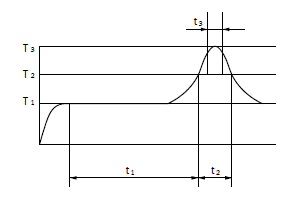
T1 = 150 to 180°C
T2 = 230°C
T3 = 240 to 250°C *
t1 = 60 to 120 s
t2 = Within 30 s
t3 = Within 10 s
* 240 to 245°C for SON, VSSOP and TSON package
(2) Other soldering methods
Other soldering methods (VPS, hot-air, hot plate, laser heating, pulse heater, etc.) affect the PhotoMOS® characteristics differently, please evaluate the device under the actual usage.
(3) Manual soldering method
Temperature: 350 to 400°C, within 3 s, electrical power 30 to 60 W
2) Example of through hole terminal recommended conditions
(1) DWS soldering method
In case of automatic soldering, following conditions should be observed. (recommended condition number of times: Max. 1 time, measurement point: soldering lead *1)
|
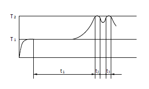
T1 = 120°C
T2 = Max. 260°C
t1 = within 60 s
t2 + t3 = within 5 s
*1 Solder temperature: Max. 260°C
(2) Other soldering method (recommended condition: 1 time)
Preheating: Max. 120°C, within 120 s, measurement point: soldering lead
Soldering: Max. 260°C, within 10 s, measurement area: soldering temperature
(3) Manual soldering method
Temperature: 350 to 400°C, within 3 s, electrical power 30 to 60 W
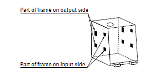
■About the exposed terminals on the sides of the package (for VSSOP)
For VSSOP type, as shown in the following figure, part of the input and output frames are exposed on the sides of the package. Due to this, please be keep in mind the cautions listed below.
- 1.Take care to avoid short circuits between exposed terminals, which may cause insulation deterioration between input and output, leading to destruction of internal elements.
- 2.Since the exposed terminals are connected electrically to the internal element, please refer to the item “■ Deterioration and destruction caused by discharge of static electricity”, and implement sufficient measures to control static electricity.
- 3.When installing the devices in the vicinity, please keep in mind that if the exposed frames of adjacent devices get too close, a short between devices may occur.
|
■Adjacent mounting
When several PhotoMOS® are mounted closely each other or heat-generating components are mounted close to the PhotoMOS®, the abnormal heating may occur. This abnormal heat may be caused by the internal element when energized or thermal interference between the devices. The degree of temperature rise depends on the mounting layout of the devices and usage condition, therefore please be sure to use PhotoMOS® with reduced load current after testing under the worst condition of the actual usage.
■Transportation and storage
- 1.Extreme vibration during transport may deform the lead or damage the PhotoMOS® characteristics. Please handle the outer and inner boxes with care.
- 2.Inadequate storage condition may degrade soldering, appearance, and characteristics. The following storage conditions are recommended:
- Temperature: 0 to 45°C
- Humidity: Max. 70% RH
- Atmosphere: No harmful gasses such as sulfurous acid gas, minimal dust.
- 3.Storage before TSON, VSSOP, SON, SSOP, or SOP processing
In case the heat stress of soldering is applied to the PhotoMOS® which absorbs moisture inside of its package, the evaporation of the moisture increases the pressure inside the package and it may cause the package blister or crack. This device is sensitive to moisture and it is packed in the sealed moisture-proof package. Please make sure the following condition after unsealing.
* Please use the device immediately after unsealing.
(Within 30 days at 0 to 30°C and Max. 70% RH)
* If the device will be kept for a long time after unsealing, please store in the another moisture-proof package containing silica gel. (Please use within 90 days.)
■Water condensation
Water condensation occurs when the ambient temperature changes suddenly from a high temperature to low temperature at high humidity, or the device is suddenly transferred from a low ambient temperature to a high temperature and humidity. Condensation causes the failures such as insulation deterioration. Panasonic Industry Co., Ltd. does not guarantee the failures caused by water condensation. The heat conduction by the equipment the PhotoMOS® is mounted may accelerate the water condensation. Please confirm that there is no condensation in the worst condition of the actual usage. (Special attention should be paid when high temperature heating parts are close to the PhotoMOS®.)
■About foreign matter between the output terminals (AQY206GV)
The distance between the output terminals of this device is short. If foreign matter is caught between the output terminals after mounting on the PC board, it will result in a leakage path. This leakage path increases the leakage current, which results in your product(s) to malfunction. Additionally, the leakage path causes abnormal heat generation and short circuiting, which results in the destruction of your product(s).
Although the absolute maximum load voltage rating is guaranteed for this device, please ensure the prevention of foreign matter on the area between the output terminals and evaluate this device in the most extreme conditions of actual usage.
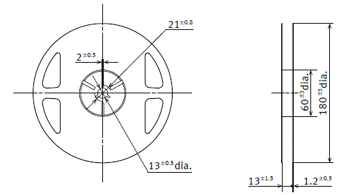
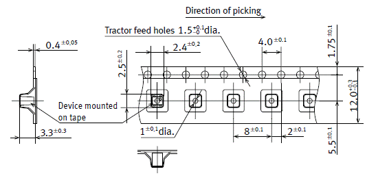
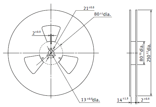
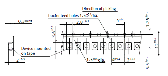
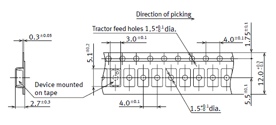
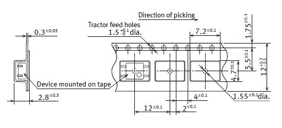
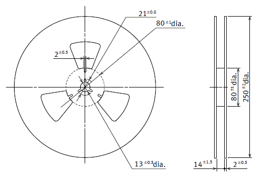
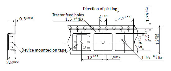
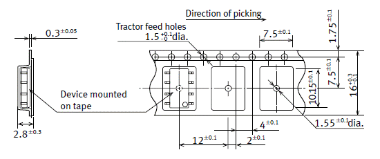
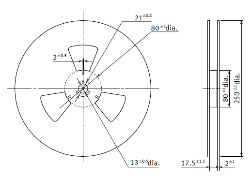
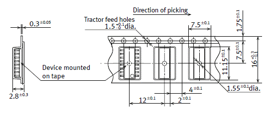
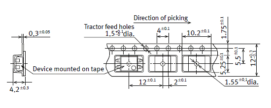
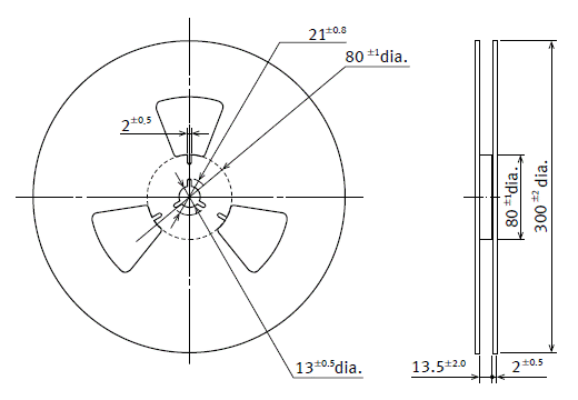
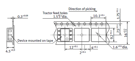
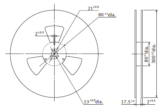
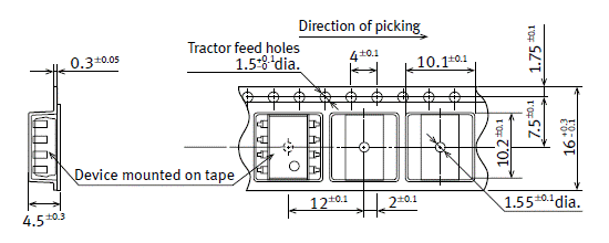
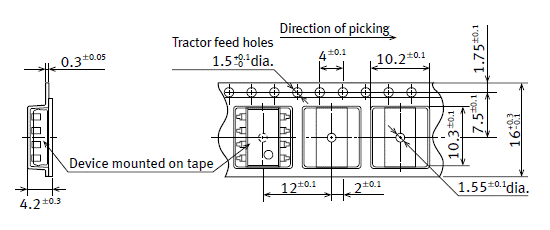
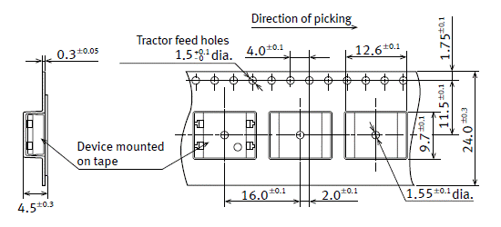
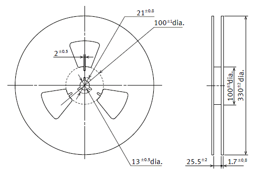
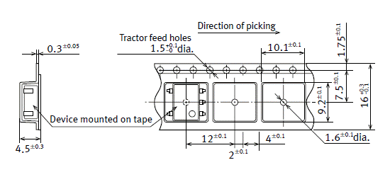
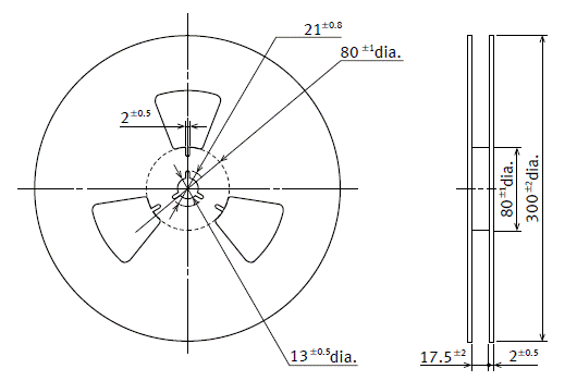
■Packing format
1.Tape and reel
| ※Click each figure to enlarge. | mm |
| Tape dimensions | Dimensions of tape reel | |
|---|---|---|
| TSON 4-pin |
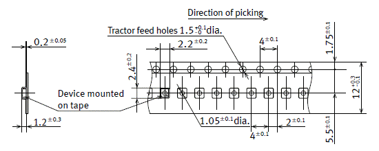
(1) When picked from 1/2-pin side: Part No. AQY2C*R*PX, AQY2C*R*P1X (Shown above) |
*Quality of material: Polystyrene (PS) |
| VSSOP 4-pin |
(1) When picked from 1 and 4-pin side: Part No. AQY*TY (Shown above) |
*Quality of material: Paper |
| SON 4-pin |
(1) When picked from 1 and 4-pin side: Part No. AQY*MY, AQY*M1Y (Shown above) |
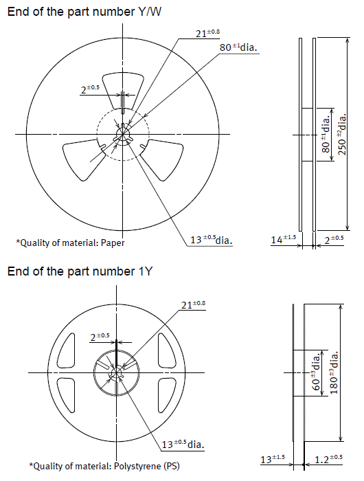
*Quality of material: Paper, Polystyrene (PS) |
| SSOP 4-pin |
(1) When picked from 1 and 4-pin side: Part No. AQY*VY, AQY221*V1Y, APV*111*VY, APV*111*V1Y (Shown above) |
|
| SOP 4-pin |
(1) When picked from 1/2-pin side: Part No. AQY*SX, APV**21SX (Shown above) |
*Quality of material: Paper |
| SOP 6-pin |
(1) When picked from 1/2/3-pin side: Part No. AQV*SX (Shown above) |
|
| SOP 8-pin |
(1) When picked from 1/2/3/4-pin side: Part No. AQW*SX (Shown above) |
*Quality of material: Paper |
| SOP 16-pin |
(1) When picked from 1/2/3/4/5/6/7/8-pin side: Part No. AQS*SX (Shown above) |
|
| DIP 4-pin Surface mount terminal |
(1) When picked from 1/2-pin side: Part No. AQY*HAX, AQY210HLAX (Shown above) |
*Quality of material: Paper |
| DIP 6-pin Surface mount terminal |
(1) When picked from 1/2/3-pin side: Part No. AQV*AX (Shown above) |
*Quality of material: Paper |
| DIP 8-pin Surface mount terminal |
(1) When picked from 1/2/3/4-pin side: Part No. AQW*AX (Shown above) |
|
| DIP 8-pin Surface mount terminal High I/O isolation voltage type |
(1) When picked from 1/2/3/4-pin side: Part No. AQW*EHAX, AQW210HLAX (Shown above) |
|
| Power-DIP 4-pin SMD |
(1) When picked from 1/2-pin side: Part No. AQY*AX (Shown above) |
*Quality of material: Paper |
| DIP 6-pin Surface mount terminal (Photovoltaic MOSFET driver) |
(1) When picked from 1/2/3-pin side: Part No. APV1122AX (Shown above) |
*Quality of material: Paper |
| Note: | Note: “ * ” indicates characters of number or alphabet. |
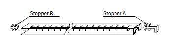
2.Tube
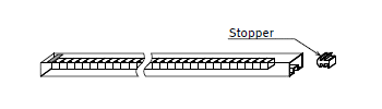
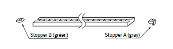
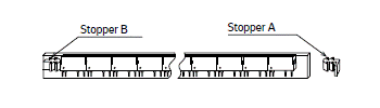
Devices are packaged in a tube so that 1-pin is on the stopper B side. Observe correct orientation when mounting them on PC boards.
|
|
|
|
■Current limit function (output current control)
- 1.Current limit function aims to increase resistance to surges when the switch is turned on. Before using this function, connect the varistor to the output as shown in the figure below.
|
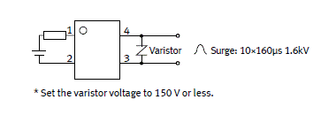
- 2.The current limit function capability can be lost if used longer than the specified time. Be sure to set the output loss to the max. rate.
■Short circuit protection circuit
The short circuit protection circuit is designed to protect circuits from excess current. Therefore, surge current may be detected as current overload in which case the output current will be cut and the off state maintained. For this reason, please include the inrush current in the load current and keep it below the maximum load current. Also, in order to maintain stability of internal IC operation, maintain an input current of at least 5 mA (Latch type), 10 mA (Non Latch type).
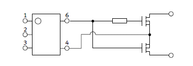
■Photovoltaic MOSFET driver cautions for use
When two external MOSFETs are connected with a common source terminal, oscillation may occur when operation is restored. Therefore, please insert a 100 to 1,000 ohms resistor between the gate terminal of the first MOSFET and the gate terminal of the second MOSFET.
A typical example of this is given in the circuit below.
|
■Input LED current (For High Capacity type: with part number G)
When making PhotoMOS turn on and turn off, please make sure that the LED forward current increases and decreases instantly.
■Input voltage (for Power voltage-sensitive type)
For rising and dropping ratio of input voltage (dv/dt), maintain Min. 100 mV/s.
■Adjacent mounting (for Power type)
- 1.When devices are mounted close together with the heatgenerated devices, ambient temperature may rise abnormally. Mounting layout and ventilation should be considered.
- 2.When many devices are mounted close together, load current should be reduced. (Refer to the data of “Load current in adjacent mounting vs. Ambient temperature characteristics.”)
■Recommended load voltage
As a guide in selecting PhotoMOS®, please refer to the following table.
1.Power photoMOS® (1 Form A)
| Absolute maximum rating | Recommended load voltage | |||
|---|---|---|---|---|
| Load voltage | Load current | |||
| DC type | AQZ102 | 60 V DC | 4.0 A DC | 5, 12, 24 V DC |
| AQZ105 | 100 V DC | 2.6 A DC | 48 V DC | |
| AQZ107 | 200 V DC | 1.3 A DC | 100 V DC | |
| AQZ104 | 400 V DC | 0.7 A DC | 200 V DC | |
| AC/DC type | AQZ202 | Peak AC, DC 60 V | Peak AC, DC 3.0 A | 12 V AC 5, 12, 24 V DC |
| AQZ205 | Peak AC, DC 100 V | Peak AC, DC 2.0 A | 24 V AC 48 V DC |
|
| AQZ207 | Peak AC, DC 200 V | Peak AC, DC 1.0 A | 48 V AC 100 V DC |
|
| AQZ204 | Peak AC, DC 400 V | Peak AC, DC 0.5 A | 120 V AC 200 V DC |
|
2.Power PhotoMOS® (1 Form B)
| Absolute maximum rating | Recommended load voltage | |||
|---|---|---|---|---|
| Load voltage | Load current | |||
| AC/DC type | AQZ404 | Peak AC, DC 400 V | Peak AC, DC 0.5 A | 100 V AC 200 V DC |
3.Power PhotoMOS® Voltage-sensitive type (1 Form A)
| Absolute maximum rating | Recommended load voltage | |||
|---|---|---|---|---|
| Load voltage | Load current | |||
| DC type | AQZ102D | 60 V DC | 3.6 A DC | 5, 12, 24 V DC |
| AQZ105D | 100 V DC | 2.3 A DC | 48 V DC | |
| AQZ107D | 200 V DC | 1.1 A DC | 100 V DC | |
| AQZ104D | 400 V DC | 0.6 A DC | 200 V DC | |
| AC/DC type | AQZ202D | Peak AC, DC 60 V | Peak AC, DC 2.7 A | 12 V AC 5, 12, 24 V DC |
| AQZ205D | Peak AC, DC 100 V | Peak AC, DC 1.8 A | 24 V AC 48 V DC |
|
| AQZ207D | Peak AC, DC 200 V | Peak AC, DC 0.9 A | 48 V AC 100 V DC |
|
| AQZ204D | Peak AC, DC 400 V | Peak AC, DC 0.45 A | 120 V AC 200 V DC |
|
4.Power PhotoMOS® High Capacity type (1 Form A)
| Absolute maximum rating | Recommended load voltage | |||
|---|---|---|---|---|
| Load voltage | Load current | |||
| DC type | AQZ192 | 60 V DC | 10 A DC | 5, 12, 24 V DC |
| AQZ197 | 200 V DC | 5 A DC | 100 V DC | |
| AC/DC type | AQZ202G | Peak AC, DC 60 V | Peak AC, DC 6 A | 12 V AC 5, 12, 24 V DC |
| AQZ205G | Peak AC, DC 100 V | Peak AC, DC 4 A | 24 V AC 48 V DC |
|
| AQZ207G | Peak AC, DC 200 V | Peak AC, DC 2 A | 48 V AC 100 V DC |
|
| AQZ206G2 | Peak AC, DC 600 V | Peak AC, DC 1 A | 120, 240 V AC 200, 400 V DC |
|
BY EMAIL
- U.S.A.
- +1-800-344-2112
- Europe
- +49-89-45354-1000
- China
- +86-10-59255988
- Singapore
- +65-6299-9181


Requests to customers (Automation Control Components & Industrial Device) [Excluding specific product]
Requests to customers (Automation Control Components & Industrial Device) [For specific product]
Requests to customers (FA Sensors & Components [Excluding motors])
Requests to customers (Dedicated to industrial motors)
- COMPONENTS & DEVICES
- FA SENSORS & COMPONENTS
- Fiber Sensors
- Photoelectric Sensors / Laser Sensors
- Micro Photoelectric Sensors
- Light Curtains / Safety Components
- Area Sensors
- Inductive Proximity Sensors
- Particular Use Sensors
- Sensor Options
- Wire-Saving Systems
- Programmable Controllers / Interface Terminal
- Human Machine Interface
- Pressure Sensors / Flow Sensors
- Measurement Sensors
- Static Control Devices
- Laser Markers / 2D Code Readers
- Machine Vision System
- Energy Management Solutions
- Timers / Counters / FA Components
- MOTORS
![]()