
 Business
> Industrial Devices
> Automation Controls Top
> Components & Devices
> Relays / Couplers
> PhotoIC Coupler
> 20 Mbps type
> Rating/Performance
Business
> Industrial Devices
> Automation Controls Top
> Components & Devices
> Relays / Couplers
> PhotoIC Coupler
> 20 Mbps type
> Rating/Performance
20 Mbps type
-
Lineup
-
 20 Mbps type
Low input voltage and low power consumption achieved. High speed Photo Coupler with receiver circuit IC.
20 Mbps type
Low input voltage and low power consumption achieved. High speed Photo Coupler with receiver circuit IC.
-
 50 Mbps type
High speed Photo Coupler with receiver circuit IC.
50 Mbps type
High speed Photo Coupler with receiver circuit IC.
-
- CAD data Catalogs/Datasheets
- FAQ
|
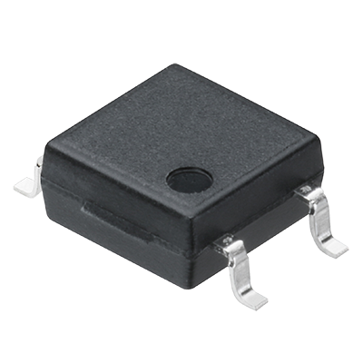
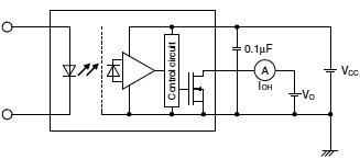
Totem pole output
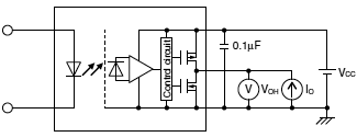
Absolute maximum ratings (Ambient temperature: 25°C)
| Item | Symbol | APS1241S | Remarks | |
|---|---|---|---|---|
| Input | LED forward current | IF | 25 mA | |
| LED reverse voltage | VR | 5 V | ||
| Peak forward current | IFP | 1 A | f = 100 Hz, Duty factor = 0.1%, 1 shot | |
| Output | Supply voltage | VCC | 6 V | |
| Output voltage | VO | 6 V | ||
| Output current | IO | 10 mA | ||
| Power dissipation | Pout | 40 mW | ||
| I/O isolation voltage | Viso | 3,750 V rms | ||
| Ambient temperature (Operating) | Topr | -40 to +105°C | (Avoid icing and condensation) | |
| Ambient temperature (Storage) | Tstg | -40 to +125°C | ||
| Junction temperature | Tj | 125°C | ||
Electrical characteristics
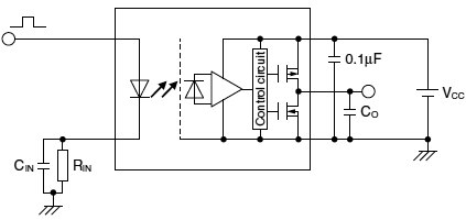
(Unless otherwise specified, Ta = -40 to +105°C, VCC = 2.7 to 5.5 V)
| Item | Symbol | APS1241S | Condition | ||
|---|---|---|---|---|---|
| Input | Threshold input current | Maximum | IFHL | 4 mA | VCC = 5 V, VO < 0.4 V |
| LED dropout voltage | Minimum | VF | 1.45 V | IF = 10 mA, Ta = 25°C | |
| Typical | 1.6 V | ||||
| Maximum | 1.8 V | ||||
| Input capacitance | Typical | Ct | 20 pF | f = 1 MHz, VB = 0 V, Ta = 25°C | |
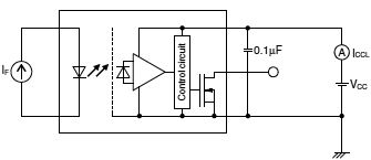
| Output | Low level supply current | Maximum | ICCL | 3 mA | IF = 9 mA |
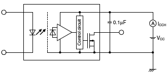
| High level supply current | Maximum | ICCH | 3 mA | IF = 0 mA | |
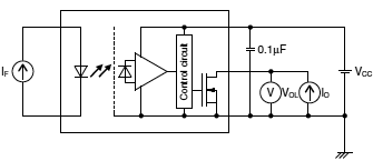
| Low level output voltage | Maximum | VOL | 0.4 V | IF = 9 mA, IO = 4 mA, Vcc = 5 V | |
| High level output voltage | Minimum | VOH | 4 V | IF = 0 mA, IO = -4 mA, Vcc = 5 V | |
| Item | Symbol | APS1241S | Condition | ||
|---|---|---|---|---|---|
| Transfer characteristics |
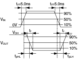
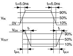
Propagation delay time (H ➝ L) |
Maximum | tpHL | 55 ns | VIN = 0 ➝ 2.5 V, RIN = 100 Ω CIN = 15 pF, CO = 15 pF |
| Propagation delay time (L ➝ H) |
Maximum | tpLH | 55 ns | VIN = 2.5 ➝ 0 V, RIN = 100 Ω CIN = 15 pF, CO = 15 pF |
|
| Propagation delay skew | Maximum | tpsk | 30 ns | - | |
| Pulse width distortion | Maximum | |tpHL-tpLH| | 30 ns | VIN = 2.5 V/10 MHz, RIN = 100 Ω CIN = 15 pF, CO = 15 pF |
|
| Output fall time | Typical | tf | 2 ns | VIN = 0 ➝ 2.5 V, RIN = 100 Ω CIN = 15 pF, CO = 15 pF |
|
| Output rise time | Typical | tr | 2 ns | VIN = 2.5 ➝ 0 V, RIN = 100 Ω CIN = 15 pF, CO = 15 pF |
|
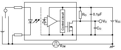
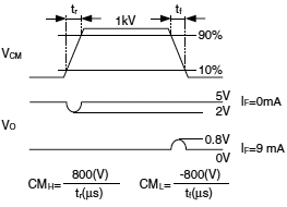
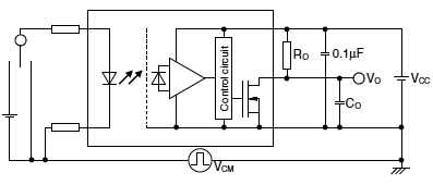
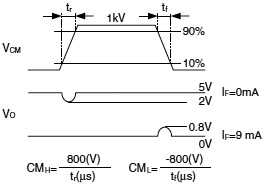
| Common mode transient immunity at low level output |
Minimum | CML | 20 kV/μs | VCM = 1000 Vp-p' , IF = 9 mA, VCC = 5 V, VO (MAX) = 0.4 V, Ta = 25°C |
|
| Common mode transient immunity at high level output |
Minimum | CMH | 20 kV/μs | VCM = 1000 Vp-p', IF = 0 mA, VCC = 5 V, VO (MIN) = 4 V, Ta = 25°C |
|
| I/O capacitance | Typical | Ciso | 0.5 pF | f = 1 MHz, VB = 0 V, Ta = 25°C | |
| Initial I/O isolation resistance | Minimum | Riso | 1000 MΩ | 500 V DC, RH ≦ 60 %, Ta = 25°C | |
|
|
||||
|
|
|
||||||
|
||||||
Recommended operating conditions
Please use under recommended operating conditions to obtain expected characteristics.
| Item | Symbol | Min. | Max. | Unit |
|---|---|---|---|---|
| LED forward current | IF | 6 | 12 | mA |
| Supply voltage | VCC | 2.7 | 5.5 | V |
| LED off voltage | VF(OFF) | 0 | 0.8 | V |
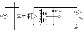
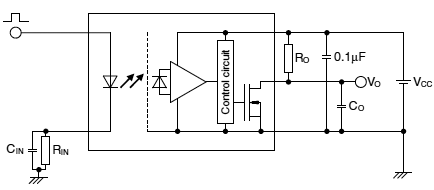
Open drain output
Absolute maximum ratings (Ambient temperature: 25°C)
| Item | Symbol | APS2241S | Remarks | |
|---|---|---|---|---|
| Input | LED forward current | IF | 25 mA | |
| LED reverse voltage | VR | 5 V | ||
| Peak forward current | IFP | 1 A | f = 100 Hz, Duty factor = 0.1%, 1 shot | |
| Output | Supply voltage | VCC | 6 V | |
| Output voltage | VO | 6 V | ||
| Output current | IO | 25 mA | ||
| Power dissipation | Pout | 40 mW | ||
| I/O isolation voltage | Viso | 3,750 Vrms | ||
| Ambient temperature (Operating) | Topr | -40 to +105°C | (Avoid icing and condensation) | |
| Ambient temperature (Storage) | Tstg | -40 to +125°C | ||
| Junction temperature | Tj | 125°C | ||
Electrical characteristics
(Unless otherwise specified, Ta = -40 to +105°C, VCC = 2.7 to 5.5 V)
| Item | Symbol | APS2241S | Condition | ||
|---|---|---|---|---|---|
| Input | Threshold input current | Maximum | IFHL | 4 mA | VCC = 5 V, VO < 0.6 V |
| LED dropout voltage | Minimum | VF | 1.45 V | IF = 10 mA, Ta = 25°C | |
| Typical | 1.6 V | ||||
| Maximum | 1.8 V | ||||
| Input capacitance | Typical | Ct | 20 pF | f = 1 MHz, VB = 0 V, Ta = 25°C | |
| Output | Low level supply current | Maximum | ICCL | 3 mA | IF = 9 mA |
| High level supply current | Maximum | ICCH | 3 mA | IF = 0 mA | |
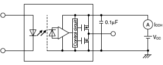
| Low level output voltage | Maximum | VOL | 0.6 V | IF = 9 mA, IO = 13 mA, Vcc = 5 V | |
| High level output current | Maximum | IOH | 50 μA | IF = 0 mA, Vcc = 5.5 V, VO = 5.5 V | |
| Item | Symbol | APS2241S | Condition | |
|---|---|---|---|---|
| Propagation delay time (H ➝ L) |
Maximum | tpHL | 60 ns | VIN = 0 ➝ 2.5 V, RIN = 100 Ω CIN = 15 pF, RO = 360 Ω, CO = 15 pF |
| Propagation delay time (L ➝ H) |
Maximum | tpLH | 60 ns | VIN = 2.5 ➝ 0 V, RIN = 100 Ω CIN = 15 pF, RO = 360 Ω, CO = 15 pF |
| Propagation delay skew | Maximum | tpsk | 40 ns | - |
| Pulse width distortion | Maximum | |tpHL-tpLH| | 35 ns | VIN = 2.5 V/5 MHz, RIN = 100 Ω CIN = 15 pF, RO = 360 Ω, CO = 15 pF |
| Output fall time | Typical | tf | 1 ns | VIN = 0 ➝ 2.5 V, RIN = 100 Ω CIN = 15 pF, RO = 360 Ω, CO = 15 pF |
| Output rise time | Typical | tr | 18 ns | VIN = 2.5 ➝ 0 V, RIN = 100 Ω CIN = 15 pF, RO = 360 Ω, CO = 15 pF |
| Common mode transient immunity at low level output |
Minimum | CML | 20 kV/μs | VCM = 1000 Vp-p', IF = 9 mA, VCC = 5 V VO (MAX) = 0.8 V, Ta = 25°C |
| Common mode transient immunity at high level output |
Minimum | CMH | 20 kV/μs | VCM = 1000 Vp-p', IF = 0 mA, VCC = 5 V VO(MIN) = 2 V, Ta = 25°C |
| I/O capacitance | Typical | Ciso | 0.5 pF | f = 1 MHz, VB = 0 V, Ta = 25°C |
| Initial I/O isolation resistance | Minimum | Riso | 1,000 MΩ | 500 V DC, RH ≦ 60 %, Ta = 25°C |
|
|
||||
|
|
|
||||||
|
||||||
Recommended operating conditions
Please use under recommended operating conditions to obtain expected characteristics.
| Item | Symbol | Min. | Max. | Unit |
|---|---|---|---|---|
| LED forward current | IF | 6 | 12 | mA |
| Supply voltage | VCC | 2.7 | 5.5 | V |
| LED off voltage | VF(OFF) | 0 | 0.8 | V |
|
Related Information
BY EMAIL
- U.S.A.
- +1-800-344-2112
- Europe
- +49-89-45354-1000
- China
- +86-10-59255988
- Singapore
- +65-6299-9181


Requests to customers (Automation Control Components & Industrial Device) [Excluding specific product]
Requests to customers (Automation Control Components & Industrial Device) [For specific product]
Requests to customers (FA Sensors & Components [Excluding motors])
Requests to customers (Dedicated to industrial motors)
- COMPONENTS & DEVICES
- FA SENSORS & COMPONENTS
- Fiber Sensors
- Photoelectric Sensors / Laser Sensors
- Micro Photoelectric Sensors
- Light Curtains / Safety Components
- Area Sensors
- Inductive Proximity Sensors
- Particular Use Sensors
- Sensor Options
- Wire-Saving Systems
- Programmable Controllers / Interface Terminal
- Human Machine Interface
- Pressure Sensors / Flow Sensors
- Measurement Sensors
- Static Control Devices
- Laser Markers / 2D Code Readers
- Machine Vision System
- Energy Management Solutions
- Timers / Counters / FA Components
- MOTORS
![]()