
 Business
> Industrial Devices
> Automation Controls Top
> Components & Devices
> Relays / Couplers
> PhotoMOS
> PhotoMOS Lineup
> PhotoMOS CC TSON 1 Form B
> Rating/Performance
Business
> Industrial Devices
> Automation Controls Top
> Components & Devices
> Relays / Couplers
> PhotoMOS
> PhotoMOS Lineup
> PhotoMOS CC TSON 1 Form B
> Rating/Performance
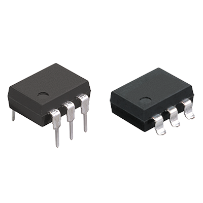
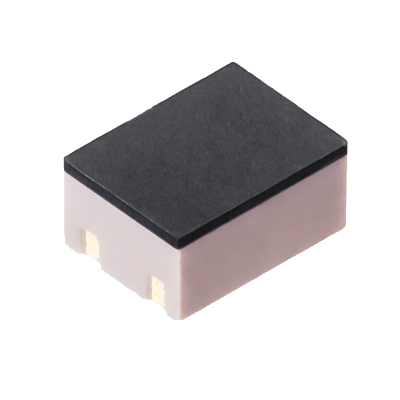
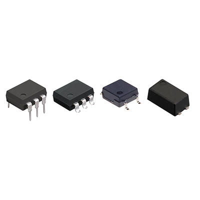
PhotoMOS CC TSON 1 Form B
-
Lineup
-
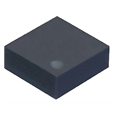 PhotoMOS CC TSON 1 Form B
Normally closed, ultra-miniature TSON type using capacitive isolation technology
PhotoMOS CC TSON 1 Form B
Normally closed, ultra-miniature TSON type using capacitive isolation technology
-
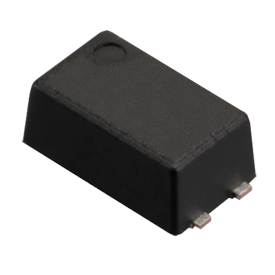
 PhotoMOS CC TSON Low CxR
Super miniature TSON package, Capacitor Coupled isolation
PhotoMOS CC TSON Low CxR
Super miniature TSON package, Capacitor Coupled isolation
-
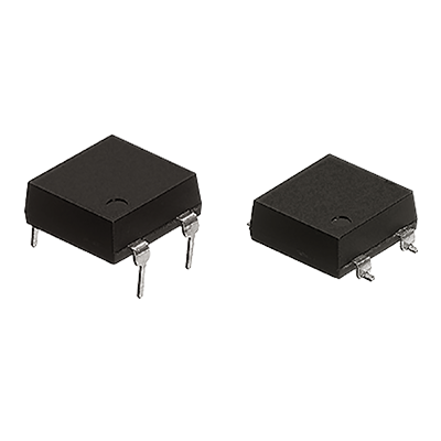
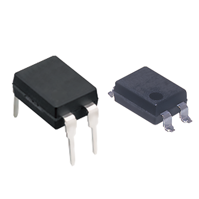 PhotoMOS GE 1 Form A (DIP4-pin type)
DIP4-pin type with high insulation
PhotoMOS GE 1 Form A (DIP4-pin type)
DIP4-pin type with high insulation
-
 PhotoMOS GE 1 Form A (DIP6-pin type)
DIP6-pin type, high insulation available
PhotoMOS GE 1 Form A (DIP6-pin type)
DIP6-pin type, high insulation available
-
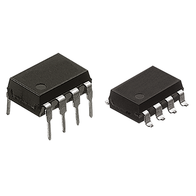
 PhotoMOS GE 1 Form A & 1 Form B
Both N.O. and N.C. contacts incorporated in a compact DIP8-pin high insulation
PhotoMOS GE 1 Form A & 1 Form B
Both N.O. and N.C. contacts incorporated in a compact DIP8-pin high insulation
-
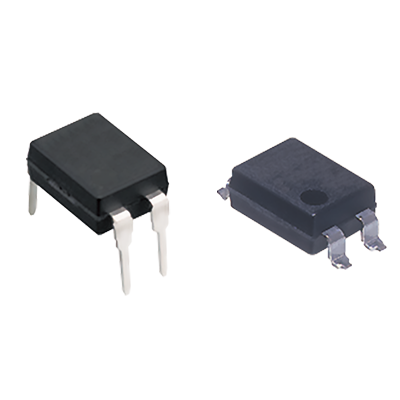 PhotoMOS GE 1 Form B (DIP4-pin type)
Normally closed type with high insulation
PhotoMOS GE 1 Form B (DIP4-pin type)
Normally closed type with high insulation
-
 PhotoMOS GE 1 Form B (DIP6-pin type)
Normally closed type with high insulation
PhotoMOS GE 1 Form B (DIP6-pin type)
Normally closed type with high insulation
-
 PhotoMOS GE 2 Form A
DIP8-pin type with high insulation
PhotoMOS GE 2 Form A
DIP8-pin type with high insulation
-
 PhotoMOS GE 2 Form B
Normally closed type with high insulation
PhotoMOS GE 2 Form B
Normally closed type with high insulation
-
 PhotoMOS GU 1 Form A (DIP6-pin type)
6-pin type for switching low-level analog signal
PhotoMOS GU 1 Form A (DIP6-pin type)
6-pin type for switching low-level analog signal
-
 PhotoMOS GU 1 Form A Current Limiting
DIP4-pin type with current limiting and high insulation
PhotoMOS GU 1 Form A Current Limiting
DIP4-pin type with current limiting and high insulation
-
 PhotoMOS GU 1 Form A High Capacity
4-pin high capacity of 1.1A, I/O isolation voltage of 5,000V
PhotoMOS GU 1 Form A High Capacity
4-pin high capacity of 1.1A, I/O isolation voltage of 5,000V
-
 PhotoMOS GU 1 Form A & 1 Form B
Both N.O. and N.C. contacts incorporated in a DIP8-pin package
PhotoMOS GU 1 Form A & 1 Form B
Both N.O. and N.C. contacts incorporated in a DIP8-pin package
-
 PhotoMOS GU 1 Form B (6-pin type)
Normally closed 6-pin type of 400V load voltage
PhotoMOS GU 1 Form B (6-pin type)
Normally closed 6-pin type of 400V load voltage
-
 PhotoMOS GU 2 Form A
Compact DIP8-pin type of 60V to 600V load voltage
PhotoMOS GU 2 Form A
Compact DIP8-pin type of 60V to 600V load voltage
-
 PhotoMOS GU 2 Form B
Normally closed DIP8-pin type of 400V load voltage
PhotoMOS GU 2 Form B
Normally closed DIP8-pin type of 400V load voltage
-
 PhotoMOS GU 1 Form A Short Circuit Protection
Short circuit protection (Non-latch type) only for DC load
PhotoMOS GU 1 Form A Short Circuit Protection
Short circuit protection (Non-latch type) only for DC load
-
 PhotoMOS GU SOP 1 Form A (4-pin)
Miniature SOP4-pin type of 60 V/100 V/350 V/400 V load voltage
PhotoMOS GU SOP 1 Form A (4-pin)
Miniature SOP4-pin type of 60 V/100 V/350 V/400 V load voltage
-
 PhotoMOS GU SOP 1 Form A (SOP6-pin type)
Miniature SOP6-pin type of 60 to 600V load voltage
PhotoMOS GU SOP 1 Form A (SOP6-pin type)
Miniature SOP6-pin type of 60 to 600V load voltage
-
 PhotoMOS GU SOP 1 Form A Current Limiting
Miniature SOP4-pin type with current limiting
PhotoMOS GU SOP 1 Form A Current Limiting
Miniature SOP4-pin type with current limiting
-
 PhotoMOS GU SOP 1 Form A High Capacity
Low on-resistance, Miniature ( SOP 4-pin ), 60 V load voltage
PhotoMOS GU SOP 1 Form A High Capacity
Low on-resistance, Miniature ( SOP 4-pin ), 60 V load voltage
-
 PhotoMOS GU SOP 1 Form A High Capacity (SOP4-pin type)
Miniature SOP4-pin type with high capacity up to Max. 1.8 A in the series
PhotoMOS GU SOP 1 Form A High Capacity (SOP4-pin type)
Miniature SOP4-pin type with high capacity up to Max. 1.8 A in the series
-
 PhotoMOS GU SOP 1 Form A High Capacity (SOP4-pin type) Low on-resistance
Low on-resistance, Miniature (SOP 4-pin), 200 V load voltage
PhotoMOS GU SOP 1 Form A High Capacity (SOP4-pin type) Low on-resistance
Low on-resistance, Miniature (SOP 4-pin), 200 V load voltage
-
 PhotoMOS GU SOP 1 Form A Short Circuit Protection
Small SOP4-pin type with short circuit protecting (Latch type)
PhotoMOS GU SOP 1 Form A Short Circuit Protection
Small SOP4-pin type with short circuit protecting (Latch type)
-
 PhotoMOS GU SOP 1 Form A & 1 Form B
Both N.O. and N.C. contacts incorporated in a small SOP8-pin package
PhotoMOS GU SOP 1 Form A & 1 Form B
Both N.O. and N.C. contacts incorporated in a small SOP8-pin package
-
 PhotoMOS GU SOP 1 Form B (SOP4-pin type)
Normally closed SOP4-pin type of 60V/350V/400V load voltage
PhotoMOS GU SOP 1 Form B (SOP4-pin type)
Normally closed SOP4-pin type of 60V/350V/400V load voltage
-
 PhotoMOS GU SOP 1 Form B (SOP6-pin type)
Normally closed SOP6-pin type of 400V load voltage
PhotoMOS GU SOP 1 Form B (SOP6-pin type)
Normally closed SOP6-pin type of 400V load voltage
-
 PhotoMOS GU SOP 2 Form A
Miniature SOP8-pin type of 60V/350V/400V load voltage
PhotoMOS GU SOP 2 Form A
Miniature SOP8-pin type of 60V/350V/400V load voltage
-
 PhotoMOS GU SOP 2 Form B
Normally closed SOP8-pin type of 400V load voltage
PhotoMOS GU SOP 2 Form B
Normally closed SOP8-pin type of 400V load voltage
-
 PhotoMOS HE 1 Form A DIP6 (5-pin)
Ideal for industrial battery monitoring system (BMS)
PhotoMOS HE 1 Form A DIP6 (5-pin)
Ideal for industrial battery monitoring system (BMS)
-
 PhotoMOS HE 1 Form A (DIP6-pin type)
DIP6-pin type with low on-resistance and high insulation
PhotoMOS HE 1 Form A (DIP6-pin type)
DIP6-pin type with low on-resistance and high insulation
-
 PhotoMOS HE 1 Form A High Capacity
Capable of Max. 3.5A high capacity load current control in the series
PhotoMOS HE 1 Form A High Capacity
Capable of Max. 3.5A high capacity load current control in the series
-
 PhotoMOS HE 1 Form A High Capacity (DIP6-pin type)
Capable of Max. 3.5 A high capacity load current control in the series
PhotoMOS HE 1 Form A High Capacity (DIP6-pin type)
Capable of Max. 3.5 A high capacity load current control in the series
-
 PhotoMOS HE 1 Form B
Normally closed DIP6-pin type Low on-resistance
PhotoMOS HE 1 Form B
Normally closed DIP6-pin type Low on-resistance
-
 PhotoMOS HE 1 Form A & 1 Form B
Both 1 Form A and 1 Form B contacts incorporated in a compact DIP8-pin with low on-resistance
PhotoMOS HE 1 Form A & 1 Form B
Both 1 Form A and 1 Form B contacts incorporated in a compact DIP8-pin with low on-resistance
-
 PhotoMOS HE 2 Form A
DIP8-pin type featuring low on-resistance with 400V load voltage
PhotoMOS HE 2 Form A
DIP8-pin type featuring low on-resistance with 400V load voltage
-
 PhotoMOS HE 2 Form B
Normally closed (2 Form B) DIP6-pin type Low on-resistance with 400V load voltage
PhotoMOS HE 2 Form B
Normally closed (2 Form B) DIP6-pin type Low on-resistance with 400V load voltage
-
 PhotoMOS HE SOP 1 Form A High Capacity
Miniature SOP6-pin type with high capacity up to Max. 3.3A in the series
PhotoMOS HE SOP 1 Form A High Capacity
Miniature SOP6-pin type with high capacity up to Max. 3.3A in the series
-
 PhotoMOS HE SOP 1 Form A High Capacity (SOP6-pin type)
Miniature SOP6-pin type with high capacity up to Max. 3 A in the series
PhotoMOS HE SOP 1 Form A High Capacity (SOP6-pin type)
Miniature SOP6-pin type with high capacity up to Max. 3 A in the series
-
 PhotoMOS HF 1 Form A
DIP6-pin type with wide variation Low on-resistance
PhotoMOS HF 1 Form A
DIP6-pin type with wide variation Low on-resistance
-
 PhotoMOS HF 1 Form A High Capacity
DIP6-pin type with 1,200 V load voltage and low on resistance (Typ. 1.0 Ω)
PhotoMOS HF 1 Form A High Capacity
DIP6-pin type with 1,200 V load voltage and low on resistance (Typ. 1.0 Ω)
-
 PhotoMOS HF SSOP 1 Form A High Capacity
Miniature SSOP package with load voltage of 600 V
PhotoMOS HF SSOP 1 Form A High Capacity
Miniature SSOP package with load voltage of 600 V
-
 PhotoMOS HS 1 Form A
DIP6-pin type featuring high sensitivity
PhotoMOS HS 1 Form A
DIP6-pin type featuring high sensitivity
-
 PhotoMOS HS SOP 1 Form A
Recommended LED forward current 2 mA, High Sensitivity (Low current-consumption)
PhotoMOS HS SOP 1 Form A
Recommended LED forward current 2 mA, High Sensitivity (Low current-consumption)
Miniature SOP4-pin Type -
 PhotoMOS PD 1 Form A
Flat Power-DIP4-pin type with high capacity up to Max. 2 A in the series.
PhotoMOS PD 1 Form A
Flat Power-DIP4-pin type with high capacity up to Max. 2 A in the series.
-
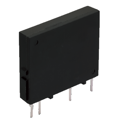
 PhotoMOS Power 1 Form A
Slim type with high capacity up to 4A DC load type in the series
PhotoMOS Power 1 Form A
Slim type with high capacity up to 4A DC load type in the series
-
 PhotoMOS Power 1 Form A High Capacity
High capacity up to Max. 6A in the series with a slim SIL package
PhotoMOS Power 1 Form A High Capacity
High capacity up to Max. 6A in the series with a slim SIL package
-
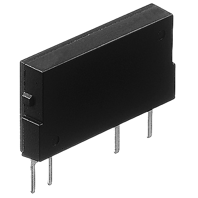
 PhotoMOS Power 1 Form A DC High Capacity
High capacity up to Max. DC10A in the series with a slim SIL package
PhotoMOS Power 1 Form A DC High Capacity
High capacity up to Max. DC10A in the series with a slim SIL package
-
 PhotoMOS Power 1 Form A Voltage-sensitive
Slim and high capacity up to 3.6 A Voltage-driven type in the series
PhotoMOS Power 1 Form A Voltage-sensitive
Slim and high capacity up to 3.6 A Voltage-driven type in the series
-
 PhotoMOS Power 1 Form B
Normally closed type in a slim SIL package Load voltage 400V
PhotoMOS Power 1 Form B
Normally closed type in a slim SIL package Load voltage 400V
-
 PhotoMOS RF SON 1 Form A CxR5
Micro-miniature SON package CxR5: 25V load voltage
PhotoMOS RF SON 1 Form A CxR5
Micro-miniature SON package CxR5: 25V load voltage
-
 PhotoMOS RF SON 1 Form A CxR10
Micro-miniature SON package CxR10: 40V load voltage
PhotoMOS RF SON 1 Form A CxR10
Micro-miniature SON package CxR10: 40V load voltage
-
 PhotoMOS RF SOP 1 Form A Low CxR
Miniature SOP4-pin type Low CxR 60V/80V load voltage
PhotoMOS RF SOP 1 Form A Low CxR
Miniature SOP4-pin type Low CxR 60V/80V load voltage
-
 PhotoMOS RF SOP 1 Form A CxR10
Miniature SOP4-pin CxR10 40V load voltage
PhotoMOS RF SOP 1 Form A CxR10
Miniature SOP4-pin CxR10 40V load voltage
-
 PhotoMOS RF 1 Form A Low on-resistance
DIP6-pin type featuring low on-resistance 200V/400V load voltage
PhotoMOS RF 1 Form A Low on-resistance
DIP6-pin type featuring low on-resistance 200V/400V load voltage
-
 PhotoMOS RF 2 Form A Low on-resistance
DIP8-pin type featuring low on-resistance 200V/400V load voltage
PhotoMOS RF 2 Form A Low on-resistance
DIP8-pin type featuring low on-resistance 200V/400V load voltage
-
 PhotoMOS RF SOP 1 Form A Low on-resistance
Miniature SOP6-pin type Low on-resistance 200V/400V load voltage
PhotoMOS RF SOP 1 Form A Low on-resistance
Miniature SOP6-pin type Low on-resistance 200V/400V load voltage
-
 PhotoMOS RF SOP 2 Form A Low on-resistance
Miniature SOP8-pin type Low on-resistance 200V load voltage
PhotoMOS RF SOP 2 Form A Low on-resistance
Miniature SOP8-pin type Low on-resistance 200V load voltage
-
 PhotoMOS RF SOP 2 Form A Low CxR
Miniature SOP8-pin type Low CxR High load voltage of 250V
PhotoMOS RF SOP 2 Form A Low CxR
Miniature SOP8-pin type Low CxR High load voltage of 250V
-
 PhotoMOS RF SOP 4 Form A Low CxR
Space-saving SOP16-pin type Low on-resistance 80V load voltage
PhotoMOS RF SOP 4 Form A Low CxR
Space-saving SOP16-pin type Low on-resistance 80V load voltage
-
 PhotoMOS RF SOP 4 Form A CxR10
Space-saving CxR type 4 channels in a SOP16-pin package
PhotoMOS RF SOP 4 Form A CxR10
Space-saving CxR type 4 channels in a SOP16-pin package
-
 PhotoMOS RF SSOP 1 Form A Low CxR
Low CxR type SSOP package 60 V, 80 V and 100 V load voltage
PhotoMOS RF SSOP 1 Form A Low CxR
Low CxR type SSOP package 60 V, 80 V and 100 V load voltage
-
 PhotoMOS RF SSOP 1 Form A CxR3
CxR3 type, SSOP package, 20 V load voltage
PhotoMOS RF SSOP 1 Form A CxR3
CxR3 type, SSOP package, 20 V load voltage
-
 PhotoMOS RF SSOP 1 Form A CxR5
Miniature SSOP CxR5: 25 V load voltage
PhotoMOS RF SSOP 1 Form A CxR5
Miniature SSOP CxR5: 25 V load voltage
-
 PhotoMOS RF SSOP 1 Form A CxR10
Miniature SSOP CxR10: 30 V/40 V load voltage
PhotoMOS RF SSOP 1 Form A CxR10
Miniature SSOP CxR10: 30 V/40 V load voltage
-
 PhotoMOS RF VSSOP 1 Form A Low CxR
Low CxR type VSSOP package 60 V and 100 V load voltage
PhotoMOS RF VSSOP 1 Form A Low CxR
Low CxR type VSSOP package 60 V and 100 V load voltage
-
 PhotoMOS RF VSSOP 1 Form A CxR3
CxR3 type, VSSOP package, 20 V load voltage
PhotoMOS RF VSSOP 1 Form A CxR3
CxR3 type, VSSOP package, 20 V load voltage
-
 PhotoMOS RF VSSOP 1 Form A CxR5
4.6 mm2 mounting area CxR5: 25 V load voltage
PhotoMOS RF VSSOP 1 Form A CxR5
4.6 mm2 mounting area CxR5: 25 V load voltage
-
 PhotoMOS RF VSSOP 1 Form A CxR10
4.6 mm2 mounting area CxR10: 30 V/40 V load voltage
PhotoMOS RF VSSOP 1 Form A CxR10
4.6 mm2 mounting area CxR10: 30 V/40 V load voltage
-
 Photovoltaic MOSFET Driver
Photovoltaic MOSFET drivers of wide variation
Photovoltaic MOSFET Driver
Photovoltaic MOSFET drivers of wide variation
-
 Photovoltaic MOSFET driver high power type
MOSFET drivers for high-speed operation and low on-resistance
Photovoltaic MOSFET driver high power type
MOSFET drivers for high-speed operation and low on-resistance
-
- CAD data Catalogs/Datasheets
- FAQ
|
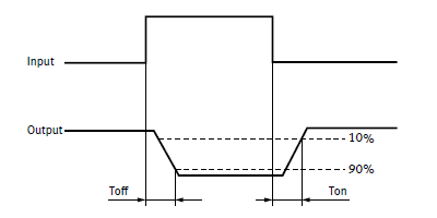
RATING
■ Absolute maximum ratings (Ambient temperature: 25°C)
| Item | Symbol | AQY4C2P | Remarks | |
|---|---|---|---|---|
| Input | Input voltage | VIN | 5.5 V | |
| Input reverse voltage | VRIN | 0.2 V | ||
| Power dissipation | Pin | 1.2 mW | ||
| Output | Load voltage (Peak AC) | VL | 60 V | |
| Continuous load current | IL | 0.15 A | Peak AC, DC | |
| Peak load current | Ipeak | 0.4 A | 100 ms (1 shot), VL = DC | |
| Power dissipation | Pout | 250 mW | ||
| Total power dissipation | PT | 250 mW | ||
| I/O isolation voltage | Viso | 200 Vrms | ||
| Ambient temperature (Operating) | Topr | -40~+105°C | (Avoid icing and condensation) | |
| Ambient temperature (Storage) | Tstg | -40~+125°C | ||
■ Electrical characteristics (Ambient temperature: 25°C)
| Item | Symbol | AQY4C2P | Condition | ||
|---|---|---|---|---|---|
| Input | Operate (OFF) voltage | Typical | VFoff |
1.6 V | IL = Max. |
| Maximum | 2.5 V | ||||
| Reverse (ON) voltage | Minimum | VFon |
0.5 V | ||
| Typical | 1.4 V | ||||
| Input current | Typical | IIN |
0.04 mA | VIN = 3.3 V | |
| Maximum | 0.1 mA | ||||
| Typical | 0.09 mA | VIN = 5 V | |||
| Maximum | 0.2 mA | ||||
| Output | On resistance | Typical | Ron |
4 Ω | VIN = 0 V, IL = Max. Within 1 s |
| Maximum | 8 Ω | ||||
| Off state leakage current | Maximum | ILeak |
10 nA | VIN = 3.3 V, VL = Max. | |
| Transfer characteristics |
Operate (OFF) time * | Typical | Toff |
0.11 ms | VIN = 0 V → 3.3 V VL = 10 V RL = 100 Ω |
| Maximum | 1.0 ms | ||||
| Typical | 0.06 ms | VIN = 0 V → 5 V VL = 10 V RL = 100 Ω |
|||
| Maximum | 0.5 ms | ||||
| Reverse (ON) time * | Typical | Ton |
0.3 ms | VIN = 3.3 V → 0 V VL = 10 V RL = 100 Ω |
|
| Maximum | 1.5 ms | ||||
| Typical | 0.5 ms | VIN = 5 V → 0 V VL = 10 V RL = 100 Ω |
|||
| Maximum | 1.5 ms | ||||
| I/O capacitance | Typical | Ciso |
1.2 pF | f = 1 MHz, VB = 0 V | |
| Maximum | 3 pF | ||||
| * | Operate/Reverse time |
|---|
|
■ Recommended operating conditions (Ambient temperature: 25°C)
Please use under recommended operating conditions to obtain expected performance. Additionally, please check the other conditions in this specification because they are affected by the actual usage. The expected performance may not be obtained due to the influence of the output waveform.
Please refer to “PhotoMOS Cautions for USE”.
| Item | Symbol | Min. | Max. | Unit | |
|---|---|---|---|---|---|
Input voltage |
VIN | 3 | 5 | V | |
| AQY4C2P | Load voltage (Peak AC) | VL | - | 30 | V |
| Continuous load current | IL | - | 0.15 | A | |
|
BY EMAIL
- U.S.A.
- +1-800-344-2112
- Europe
- +49-89-45354-1000
- China
- +86-10-59255988
- Singapore
- +65-6299-9181


Requests to customers (Automation Control Components & Industrial Device) [Excluding specific product]
Requests to customers (Automation Control Components & Industrial Device) [For specific product]
Requests to customers (FA Sensors & Components [Excluding motors])
Requests to customers (Dedicated to industrial motors)
- COMPONENTS & DEVICES
- FA SENSORS & COMPONENTS
- Fiber Sensors
- Photoelectric Sensors / Laser Sensors
- Micro Photoelectric Sensors
- Light Curtains / Safety Components
- Area Sensors
- Inductive Proximity Sensors
- Particular Use Sensors
- Sensor Options
- Wire-Saving Systems
- Programmable Controllers / Interface Terminal
- Human Machine Interface
- Pressure Sensors / Flow Sensors
- Measurement Sensors
- Static Control Devices
- Laser Markers / 2D Code Readers
- Machine Vision System
- Energy Management Solutions
- Timers / Counters / FA Components
- MOTORS
![]()