
 Business
> Industrial Devices
> Automation Controls Top
> Components & Devices
> Switches
> Light Touch Switches
> Light Touch Switches Lineup
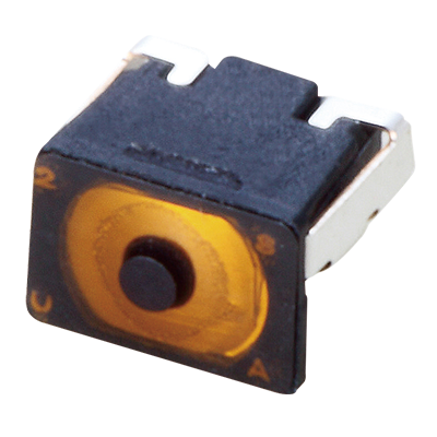
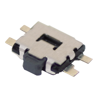
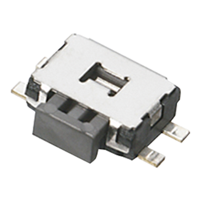
> 3.0mm x 2.6mm 2 terminals SMD (EVPBA)
> Dimensions
Business
> Industrial Devices
> Automation Controls Top
> Components & Devices
> Switches
> Light Touch Switches
> Light Touch Switches Lineup
> 3.0mm x 2.6mm 2 terminals SMD (EVPBA)
> Dimensions
3.0mm x 2.6mm 2 terminals SMD (EVPBA)
-
Lineup
-
 2.6mm x 1.6mm SMD
Low profile (0.5 to 0.53mm) and Small size (2.6 x 1.6mm). IP67
2.6mm x 1.6mm SMD
Low profile (0.5 to 0.53mm) and Small size (2.6 x 1.6mm). IP67
-
 2.8mm x 1.9mm SMD
Low profile (0.53mm to 0.60mm) and Small size (2.8 x 1.9mm). IP67
2.8mm x 1.9mm SMD
Low profile (0.53mm to 0.60mm) and Small size (2.8 x 1.9mm). IP67
-
 2.8mm x 2.3mm Side-operational Edge Mount
Side operational type with small size and improved soldering strength in operationg direction.
2.8mm x 2.3mm Side-operational Edge Mount
Side operational type with small size and improved soldering strength in operationg direction.
-
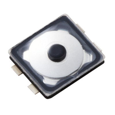
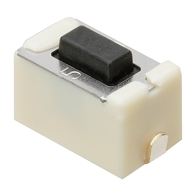
 3.0mm x 2.0mm SMD
Low profile (0.6mm) and Small size (3.0 x 2.0mm). IP67
3.0mm x 2.0mm SMD
Low profile (0.6mm) and Small size (3.0 x 2.0mm). IP67
-
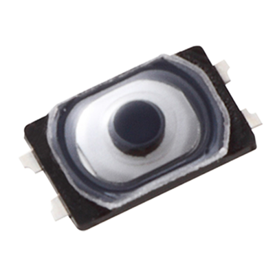
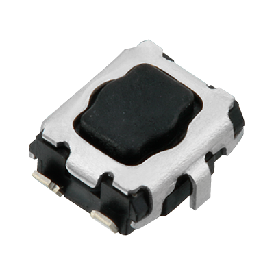
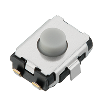
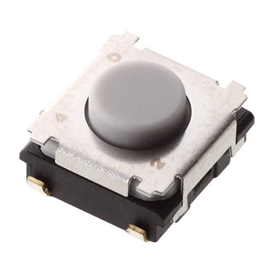
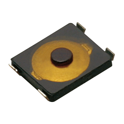 3.0mm x 2.6mm SMD
Low profile (0.65mm) and Small size (3.0 x 2.6mm).
3.0mm x 2.6mm SMD
Low profile (0.65mm) and Small size (3.0 x 2.6mm).
-
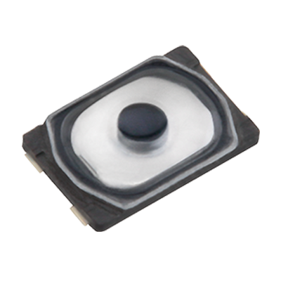
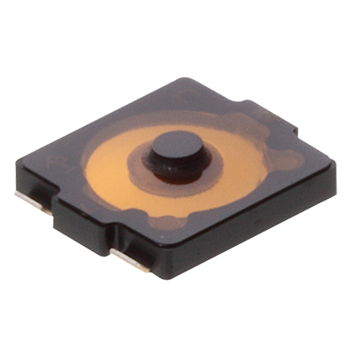
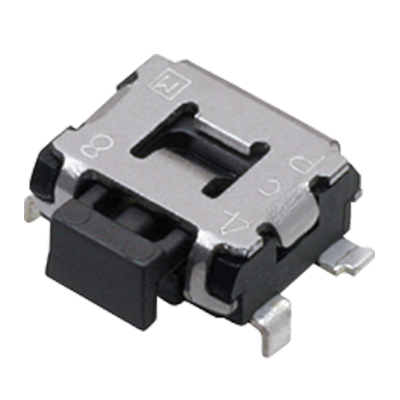
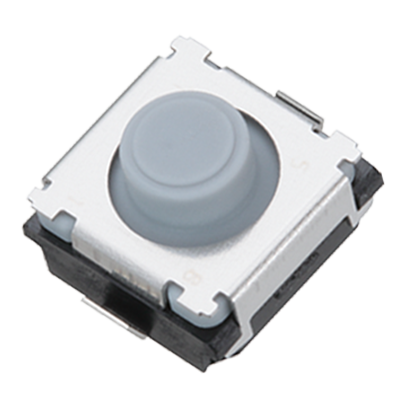
 3.0mm x 2.6mm Double-action SMD
Double action with small size.
3.0mm x 2.6mm Double-action SMD
Double action with small size.
-
 3.4mm x 2.9mm SMD
Low profile (0.7mm) and Small size (3.4 x 2.9mm). IP67
3.4mm x 2.9mm SMD
Low profile (0.7mm) and Small size (3.4 x 2.9mm). IP67
-
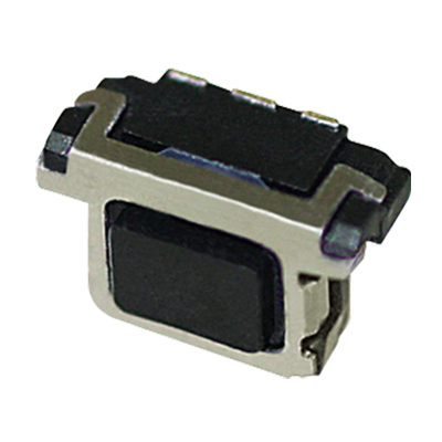
 3.4mm x 1.7mm Side-operational Edge Mount
Side operational type with small size and improved soldering strength in operationg direction. IP67
3.4mm x 1.7mm Side-operational Edge Mount
Side operational type with small size and improved soldering strength in operationg direction. IP67
-
 3.5mm x 2.9mm SMD
High operating force. With a ground terminal type available.
3.5mm x 2.9mm SMD
High operating force. With a ground terminal type available.
-
 3.5mm x 2.9mm Side-operational SMD
External dimensions: 3.5 x 2.9mm. Wide variety of terminal shape. Enhanced push plate strength performance.
3.5mm x 2.9mm Side-operational SMD
External dimensions: 3.5 x 2.9mm. Wide variety of terminal shape. Enhanced push plate strength performance.
-
 3.5mm x 2.9mm Side-operational Half Dive/SMD
Side operational type with low profile. Half dive mount with 0.7mm height from PCB surface.
3.5mm x 2.9mm Side-operational Half Dive/SMD
Side operational type with low profile. Half dive mount with 0.7mm height from PCB surface.
-
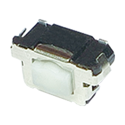
 3.8mm x 1.9mm Side-operational SMD
Side operational type (External dimensions: 3.9 x 2.05mm). IP67
3.8mm x 1.9mm Side-operational SMD
Side operational type (External dimensions: 3.9 x 2.05mm). IP67
-
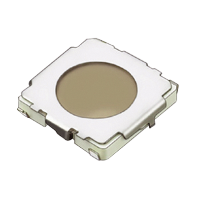
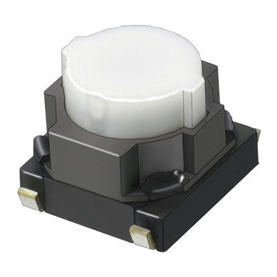
 4mm Square SMD
External dimensions: 4.1 x 4.1mm. Wide product variety. (With/Without a push plate, and with a ground terminal type available.)
4mm Square SMD
External dimensions: 4.1 x 4.1mm. Wide product variety. (With/Without a push plate, and with a ground terminal type available.)
-
 4.5mm x 2.2mm Side-operational Edge Mount
Side operational type with small size and improved soldering strength in operationg direction. Electrostatic countermeasure performance.
4.5mm x 2.2mm Side-operational Edge Mount
Side operational type with small size and improved soldering strength in operationg direction. Electrostatic countermeasure performance.
-
 4.7mm x 3.5mm SMD
High operating force and Long operational life.
4.7mm x 3.5mm SMD
High operating force and Long operational life.
-
 4.9mm x 4.0mm SMD
Achieved Long operation travel 0.23mm with low profile package 0.63mm
4.9mm x 4.0mm SMD
Achieved Long operation travel 0.23mm with low profile package 0.63mm
-
 4.9mm Square SMD
External dimensions: 4.9 x 4.9mm. With/Without a push plate type available.
4.9mm Square SMD
External dimensions: 4.9 x 4.9mm. With/Without a push plate type available.
-
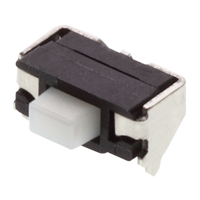
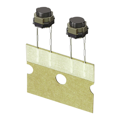
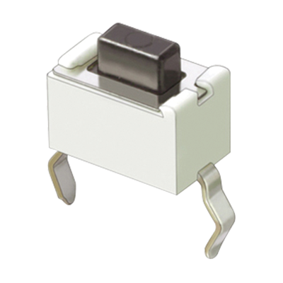 6.0mm x 3.5mm
External dimensions: 6.0 x 3.5mm. Vertical operational type with snap-in terminals.
6.0mm x 3.5mm
External dimensions: 6.0 x 3.5mm. Vertical operational type with snap-in terminals.
-
 6.0mm x 3.5mm SMD
Surface mount type (External dimensins: 6.0 x 3.5mm).
6.0mm x 3.5mm SMD
Surface mount type (External dimensins: 6.0 x 3.5mm).
-
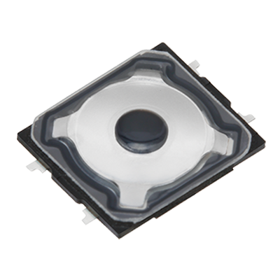
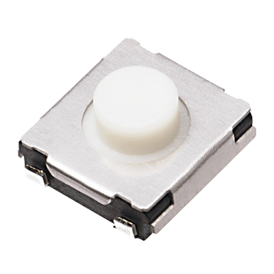 6mm Square Thin Type SMD
External dimensions: 6.5 x 6.0mm. With over travel function available.
6mm Square Thin Type SMD
External dimensions: 6.5 x 6.0mm. With over travel function available.
-
 6mm Square Middle Travel SMD
Middle travel feeling
6mm Square Middle Travel SMD
Middle travel feeling
-
 6mm Square Middle Travel 2 terminals SMD
Middle travel type with two terminal structure.
6mm Square Middle Travel 2 terminals SMD
Middle travel type with two terminal structure.
-
 6mm Square Long Travel 2R
Long travel type with radial tape.
6mm Square Long Travel 2R
Long travel type with radial tape.
-
 6mm Square Long Travel 2 terminals SMD
Long travel type with two terminal structure.
6mm Square Long Travel 2 terminals SMD
Long travel type with two terminal structure.
-
 6mm Square Long Travel SMD
External dimensions: 6.0 x 6.1mm. Long travel type.
6mm Square Long Travel SMD
External dimensions: 6.0 x 6.1mm. Long travel type.
-
 6.2mm x 2.5mm Side-operational Edge Mount
Side operational type with small size and improved soldering strength in operationg direction. High operating force performance.
6.2mm x 2.5mm Side-operational Edge Mount
Side operational type with small size and improved soldering strength in operationg direction. High operating force performance.
-
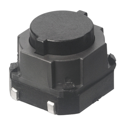 8mm Square Long Travel SMD
Prevent incorrect operation with high operating force.
8mm Square Long Travel SMD
Prevent incorrect operation with high operating force.
-
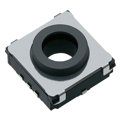 10 mm Square Center Space Long Travel SMD
Center space structure and surface mount type.
10 mm Square Center Space Long Travel SMD
Center space structure and surface mount type.
-
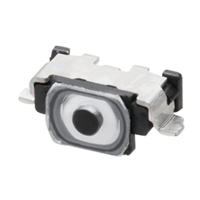
 Small-sized Side-operational SMD
Side operational type (External dimensions: 4.7 x 3.5mm).
Small-sized Side-operational SMD
Side operational type (External dimensions: 4.7 x 3.5mm).
-
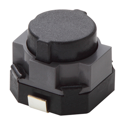
 Over Travel
Comfortable for long hours of operation thanks to over travel function.
Over Travel
Comfortable for long hours of operation thanks to over travel function.
-
- CAD data Catalogs/Datasheets
- FAQ
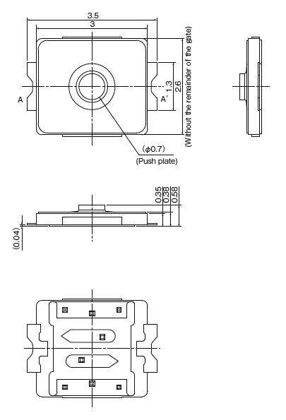
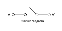
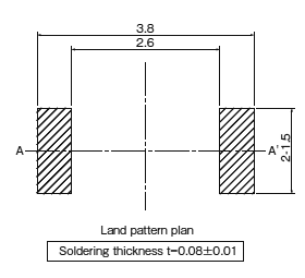
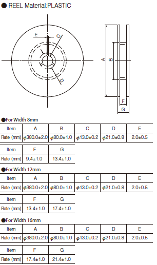
1.Dimensions in mm
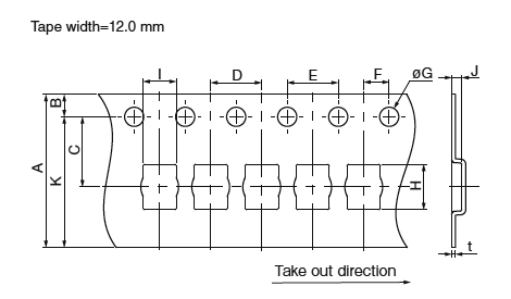
EVPBA
(Embossed Taping)
|
|
|
2.Recommended Reflow Soldering Conditions
|
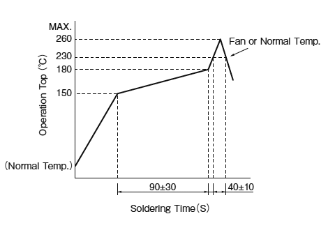
|
|

|
Related Information
CONTACT US
If you have any questions, please select the option below to contact us or find answers.
CONTACT US
BY EMAIL
BY EMAIL
Please click your area to select country or region


Related Information
Service & Support
Requests to customers (Automation Control Components & Industrial Device) [Excluding specific product]
Requests to customers (Automation Control Components & Industrial Device) [For specific product]
Requests to customers (FA Sensors & Components [Excluding motors])
Requests to customers (Dedicated to industrial motors)
- COMPONENTS & DEVICES
- FA SENSORS & COMPONENTS
- Fiber Sensors
- Photoelectric Sensors / Laser Sensors
- Micro Photoelectric Sensors
- Light Curtains / Safety Components
- Area Sensors
- Inductive Proximity Sensors
- Particular Use Sensors
- Sensor Options
- Wire-Saving Systems
- Programmable Controllers / Interface Terminal
- Human Machine Interface
- Pressure Sensors / Flow Sensors
- Measurement Sensors
- Static Control Devices
- Laser Markers / 2D Code Readers
- Machine Vision System
- Energy Management Solutions
- Timers / Counters / FA Components
- MOTORS
![]()