
 Business
> Industrial Devices
> Automation Controls Top
> FA Sensors & Components
> Static Control Devices
> Static Control Devices
> Thin-type Ionizer ER-VW
> I/O Circuit and Wiring diagrams
Business
> Industrial Devices
> Automation Controls Top
> FA Sensors & Components
> Static Control Devices
> Static Control Devices
> Thin-type Ionizer ER-VW
> I/O Circuit and Wiring diagrams
Thin-type Ionizer ER-VW
|
I/O Circuit and Wiring diagrams
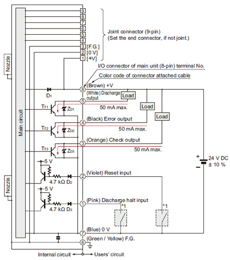
I/O circuit diagram
|
|
| Symbols・・・ | D1 : Reverse supply polarity protection diode D2, D3 : Input protection diode ZD1, ZD2, ZD3 : Surge absorption zener diode Tr1, Tr2, Tr3 : NPN output transistor |
|---|
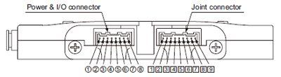
Connector terminal arrangement
|
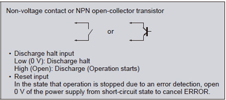
Input signal condition
|
|
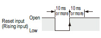
Note:
Repeated control using “Discharge halt input” input should be carried out at 1 Hz or less.
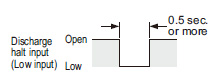
Continuous discharging for 2 sec. or more is required for stable sensing of check output.
If using with repeated control operations that include discharges of 2 sec. or less, use continuous discharges of 2 sec. or more to check the check output when carrying out maintenance.
BY EMAIL


Requests to customers (Automation Control Components & Industrial Device) [Excluding specific product]
Requests to customers (Automation Control Components & Industrial Device) [For specific product]
Requests to customers (FA Sensors & Components [Excluding motors])
Requests to customers (Dedicated to industrial motors)
- COMPONENTS & DEVICES
- FA SENSORS & COMPONENTS
- Fiber Sensors
- Photoelectric Sensors / Laser Sensors
- Micro Photoelectric Sensors
- Light Curtains / Safety Components
- Area Sensors
- Inductive Proximity Sensors
- Particular Use Sensors
- Sensor Options
- Wire-Saving Systems
- Programmable Controllers / Interface Terminal
- Human Machine Interface
- Pressure Sensors / Flow Sensors
- Measurement Sensors
- Static Control Devices
- Laser Markers / 2D Code Readers
- Machine Vision System
- Energy Management Solutions
- Timers / Counters / FA Components
- MOTORS
![]()