[System Maintenance Notice]
Due to ongoing system maintenance, the site search and specification search functions are temporarily unavailable. We apologize for any inconvenience this may cause and appreciate your understanding.
【Notification of Manufacturer Change for Panasonic Industrial Devices SUNX Products and Panasonic Industrial Devices SUNX Tatsuno Products】
From April 1, 2024, the terms "Panasonic Industrial Devices SUNX Co., Ltd." and "Panasonic Industrial Devices SUNX Tatsuno Co., Ltd."
in this page and in the manuals and other documents to be downloaded will all be replaced with "Panasonic Industry Co., Ltd." and applied accordingly.
Compact Size Picking Sensor NA1-PK3
I/O Circuit and Wiring diagrams
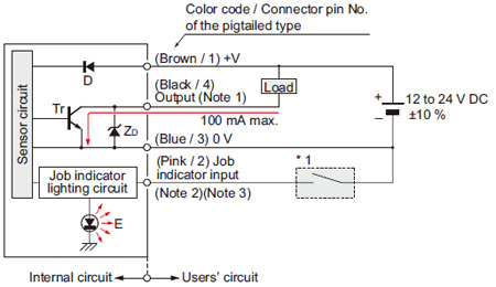
NPN output type
I/O circuit diagram
Notes:
| 1) |
The emitter does not incorporate the output (black). |
| 2) |
If a mating cable is connected to the pigtailed type, then the lead wire color is “white”. |
| 3) |
When the job indicator is used as a large size operation indicator, connect the job indicator input wire (pink) of the emitter and the receiver to the output wire (black) of the receiver. |
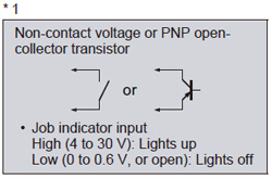
| Symbols・・・ |
D : Reserve supply polarity protection diode
ZD: Surge absorption zener diode
Tr : NPN output transistor
E : Job indicator (IND.) |
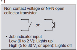
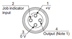
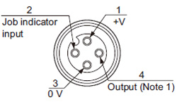
Connector pin position (Pigtailed type)
Notes:
| 1) |
No connection is required for the emitter. |
| 2) |
The pin position for the SL-WY Y-shaped connector (optional) is identical to the receiver. |
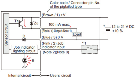
PNP output type
I/O circuit diagram
Notes:
| 1) |
The emitter does not incorporate the output (black). |
| 2) |
If a mating cable is connected to the pigtailed type, then the lead wire color is “white”. |
| 3) |
When the job indicator is used as a large size operation indicator, connect the job indicator input wire pink) of the emitter and the receiver to the output wire (black) of the receiver. |
| Symbols・・・ |
D : Reserve supply polarity protection diode
ZD: Surge absorption zener diode
Tr: PNP output transistor
E : Job indicator (IND.) |
Connector pin position (Pigtailed type)
Notes:
| 1) |
No connection is required for the emitter. |
| 2) |
The pin position for the SL-WY Y-shaped connector (optional) is identical to the receiver. |
Return to top
Return to top

 Business
> Industrial Devices
> Automation Controls Top
> FA Sensors & Components
> Sensors
> Area Sensors
> Compact Size Picking Sensor NA1-PK3
> I/O Circuit and Wiring diagrams
Business
> Industrial Devices
> Automation Controls Top
> FA Sensors & Components
> Sensors
> Area Sensors
> Compact Size Picking Sensor NA1-PK3
> I/O Circuit and Wiring diagrams