[System Maintenance Notice]
Due to ongoing system maintenance, the site search and specification search functions are temporarily unavailable. We apologize for any inconvenience this may cause and appreciate your understanding.

 Business
> Industrial Devices
> Automation Controls Top
> Components & Devices
> Switches
> Tactile Switches (Light Touch Switches)
> Tactile Switches (Light Touch Switches) Lineup
> 3.0mm x 2.0mm SMD (EVPAW, EVP6A)
> Dimensions
Business
> Industrial Devices
> Automation Controls Top
> Components & Devices
> Switches
> Tactile Switches (Light Touch Switches)
> Tactile Switches (Light Touch Switches) Lineup
> 3.0mm x 2.0mm SMD (EVPAW, EVP6A)
> Dimensions
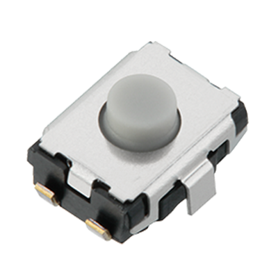
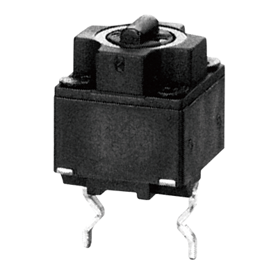
3.0mm x 2.0mm SMD (EVPAW, EVP6A)
-
Lineup
-
 2.6mm x 1.6mm SMD
Low profile (0.5 to 0.53mm) and Small size (2.6 x 1.6mm). IP67
2.6mm x 1.6mm SMD
Low profile (0.5 to 0.53mm) and Small size (2.6 x 1.6mm). IP67
-
 2.8mm x 1.9mm SMD
Low profile (0.53mm to 0.60mm) and Small size (2.8 x 1.9mm). IP67
2.8mm x 1.9mm SMD
Low profile (0.53mm to 0.60mm) and Small size (2.8 x 1.9mm). IP67
-
 2.8mm x 2.3mm Side-operational Edge Mount
Side operational type with small size and improved soldering strength in operationg direction.
2.8mm x 2.3mm Side-operational Edge Mount
Side operational type with small size and improved soldering strength in operationg direction.
-
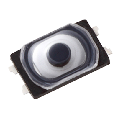
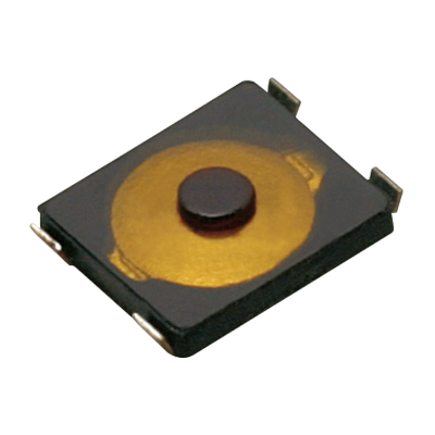
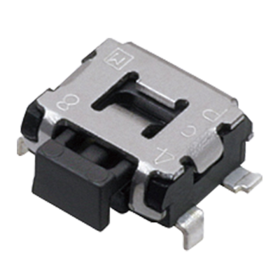
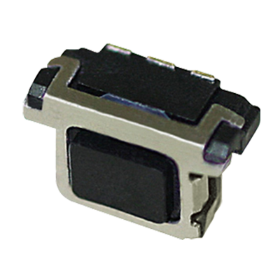
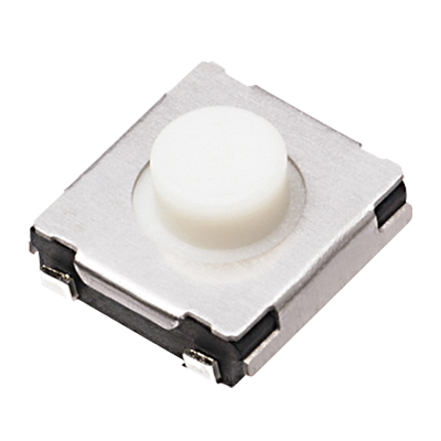
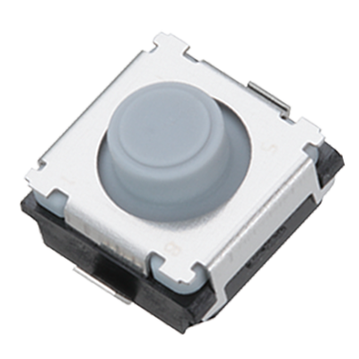
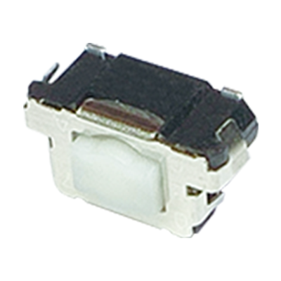
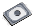
 3.0mm x 2.0mm SMD
Low profile (0.6mm) and Small size (3.0 x 2.0mm). IP67
3.0mm x 2.0mm SMD
Low profile (0.6mm) and Small size (3.0 x 2.0mm). IP67
-
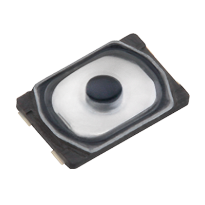
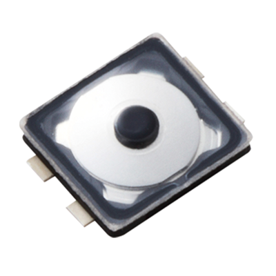
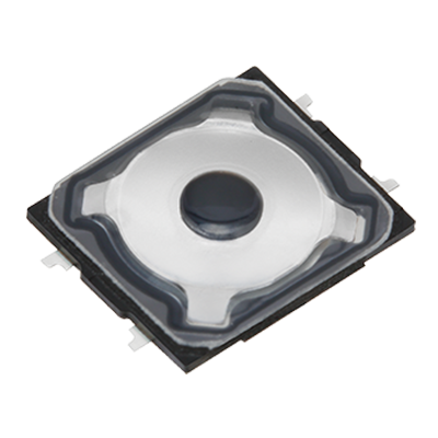
 3.0mm x 2.6mm SMD
Low profile (0.65mm) and Small size (3.0 x 2.6mm).
3.0mm x 2.6mm SMD
Low profile (0.65mm) and Small size (3.0 x 2.6mm).
-
 3.0mm x 2.6mm Double-action SMD
Double action with small size.
3.0mm x 2.6mm Double-action SMD
Double action with small size.
-
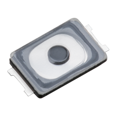
 3.4mm x 2.9mm SMD
Low profile (0.7mm) and Small size (3.4 x 2.9mm). IP67
3.4mm x 2.9mm SMD
Low profile (0.7mm) and Small size (3.4 x 2.9mm). IP67
-
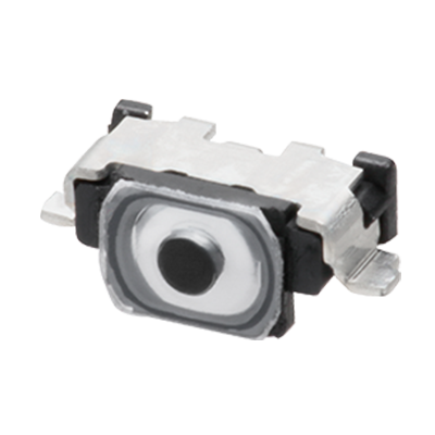 3.4mm x 1.7mm Side-operational Edge Mount
Side operational type with small size and improved soldering strength in operationg direction. IP67
3.4mm x 1.7mm Side-operational Edge Mount
Side operational type with small size and improved soldering strength in operationg direction. IP67
-
 3.5mm x 2.9mm SMD
High operating force. With a ground terminal type available.
3.5mm x 2.9mm SMD
High operating force. With a ground terminal type available.
-
 3.5mm x 2.9mm Side-operational SMD
External dimensions: 3.5 x 2.9mm. Wide variety of terminal shape. Enhanced push plate strength performance.
3.5mm x 2.9mm Side-operational SMD
External dimensions: 3.5 x 2.9mm. Wide variety of terminal shape. Enhanced push plate strength performance.
-
 3.5mm x 2.9mm Side-operational Half Dive/SMD
Side operational type with low profile. Half dive mount with 0.7mm height from PCB surface.
3.5mm x 2.9mm Side-operational Half Dive/SMD
Side operational type with low profile. Half dive mount with 0.7mm height from PCB surface.
-
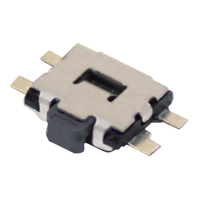
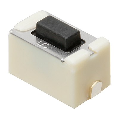
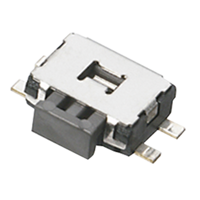
 3.8mm x 1.9mm Side-operational SMD
Side operational type (External dimensions: 3.9 x 2.05mm). IP67
3.8mm x 1.9mm Side-operational SMD
Side operational type (External dimensions: 3.9 x 2.05mm). IP67
-
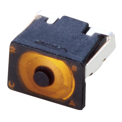
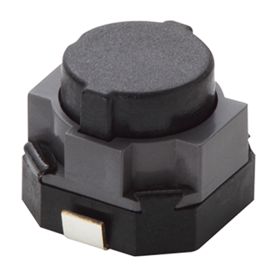
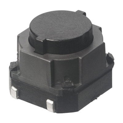
 4mm Square SMD
External dimensions: 4.1 x 4.1mm. Wide product variety. (With/Without a push plate, and with a ground terminal type available.)
4mm Square SMD
External dimensions: 4.1 x 4.1mm. Wide product variety. (With/Without a push plate, and with a ground terminal type available.)
-
 4.5mm x 2.2mm Side-operational Edge Mount
Side operational type with small size and improved soldering strength in operationg direction. Electrostatic countermeasure performance.
4.5mm x 2.2mm Side-operational Edge Mount
Side operational type with small size and improved soldering strength in operationg direction. Electrostatic countermeasure performance.
-
 4.7mm x 3.5mm SMD
High operating force and Long operational life.
4.7mm x 3.5mm SMD
High operating force and Long operational life.
-
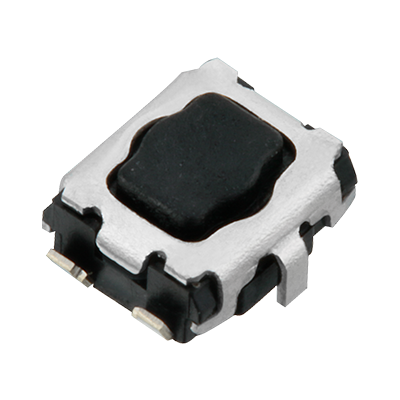
 4.9mm x 4.0mm SMD
Achieved Long operation travel 0.23mm with low profile package 0.63mm
4.9mm x 4.0mm SMD
Achieved Long operation travel 0.23mm with low profile package 0.63mm
-
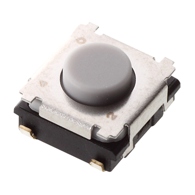
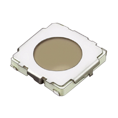 4.9mm Square SMD
External dimensions: 4.9 x 4.9mm. With/Without a push plate type available.
4.9mm Square SMD
External dimensions: 4.9 x 4.9mm. With/Without a push plate type available.
-
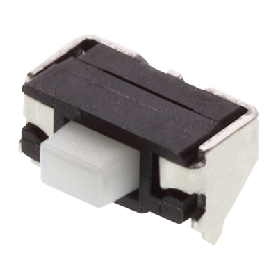
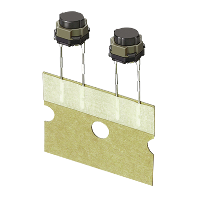
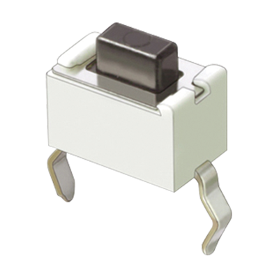 6.0mm x 3.5mm
External dimensions: 6.0 x 3.5mm. Vertical operational type with snap-in terminals.
6.0mm x 3.5mm
External dimensions: 6.0 x 3.5mm. Vertical operational type with snap-in terminals.
-
 6.0mm x 3.5mm SMD
Surface mount type (External dimensins: 6.0 x 3.5mm).
6.0mm x 3.5mm SMD
Surface mount type (External dimensins: 6.0 x 3.5mm).
-
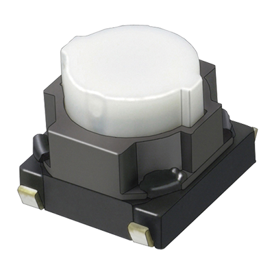
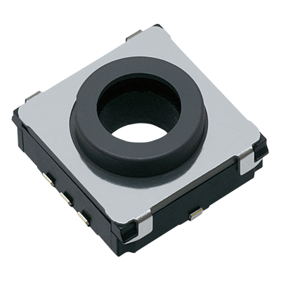
 6mm Square Thin Type SMD
External dimensions: 6.5 x 6.0mm. With over travel function available.
6mm Square Thin Type SMD
External dimensions: 6.5 x 6.0mm. With over travel function available.
-
 6mm Square Middle Travel SMD
Middle travel feeling
6mm Square Middle Travel SMD
Middle travel feeling
-
 6mm Square Middle Travel 2 terminals SMD
Middle travel type with two terminal structure.
6mm Square Middle Travel 2 terminals SMD
Middle travel type with two terminal structure.
-
 6mm Square Long Travel 2R
Long travel type with radial tape.
6mm Square Long Travel 2R
Long travel type with radial tape.
-
 6mm Square Long Travel 2 terminals SMD
Long travel type with two terminal structure.
6mm Square Long Travel 2 terminals SMD
Long travel type with two terminal structure.
-
 6mm Square Long Travel SMD
External dimensions: 6.0 x 6.1mm. Long travel type.
6mm Square Long Travel SMD
External dimensions: 6.0 x 6.1mm. Long travel type.
-
 6.2mm x 2.5mm Side-operational Edge Mount
Side operational type with small size and improved soldering strength in operationg direction. High operating force performance.
6.2mm x 2.5mm Side-operational Edge Mount
Side operational type with small size and improved soldering strength in operationg direction. High operating force performance.
-
 8mm Square Long Travel SMD
Prevent incorrect operation with high operating force.
8mm Square Long Travel SMD
Prevent incorrect operation with high operating force.
-
 10 mm Square Center Space Long Travel SMD
Center space structure and surface mount type.
10 mm Square Center Space Long Travel SMD
Center space structure and surface mount type.
-
 Small-sized Side-operational SMD
Side operational type (External dimensions: 4.7 x 3.5mm).
Small-sized Side-operational SMD
Side operational type (External dimensions: 4.7 x 3.5mm).
-
 Over Travel
Comfortable for long hours of operation thanks to over travel function.
Over Travel
Comfortable for long hours of operation thanks to over travel function.
-
- CAD data Catalogs/Datasheets
- FAQ
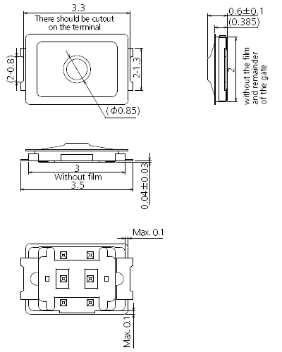
- Unit : mm
1.DIMENSIONS
EVPAW
EVP6A
(Embossed Taping)
|
|
|
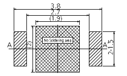
 : Recommended land pattern area
 : No soldering area
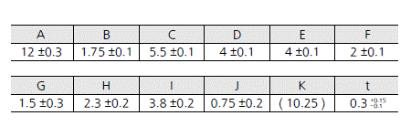
2.EMBOSSED TAPE DIMENSIONS
|
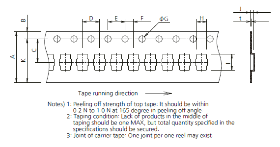
|
Related Information
BY EMAIL
- U.S.A.
- +1-800-344-2112
- Europe
- +49-89-45354-1000
- China
- +86-10-59255988
- Singapore
- +65-6299-9181


Requests to customers (Automation Control Components & Industrial Device) [Excluding specific product]
Requests to customers (Automation Control Components & Industrial Device) [For specific product]
Requests to customers (FA Sensors & Components [Excluding motors])
Requests to customers (Dedicated to industrial motors)
- COMPONENTS & DEVICES
- FA SENSORS & COMPONENTS
- Fiber Sensors
- Photoelectric Sensors / Laser Sensors
- Micro Photoelectric Sensors
- Light Curtains / Safety Components
- Area Sensors
- Inductive Proximity Sensors
- Particular Use Sensors
- Sensor Options
- Wire-Saving Systems
- Programmable Controllers / Interface Terminal
- Human Machine Interface
- Pressure Sensors / Flow Sensors
- Measurement Sensors
- Static Control Devices
- Laser Markers / 2D Code Readers
- Machine Vision System
- Energy Management Solutions
- Timers / Counters / FA Components
- MOTORS
![]()