


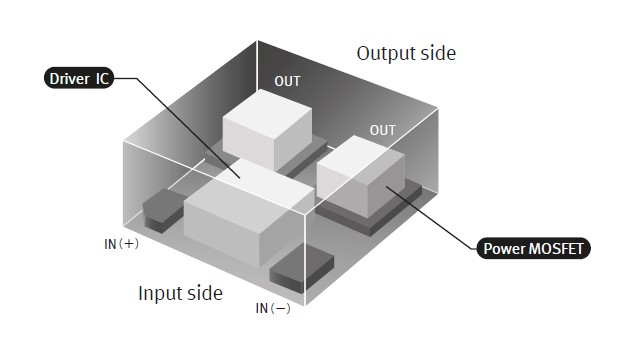
What is PhotoMOS?
A PhotoMOS is a semiconductor device with an LED as an input and MOSFET as an output.
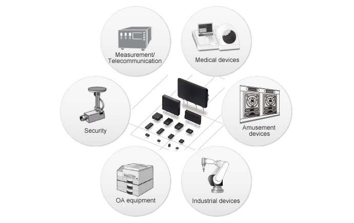
It is used in various fields to improve device reliability and reduce size.
Basic Structure
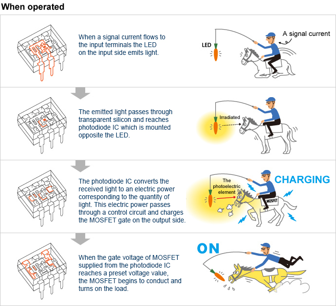
<Optical Isolation>


<Capacitor Coupled Isolation>
[Glossary]
| Epoxy | ----- | Epoxy resin |
| LED | ----- | Light Emitting Diode |
| MOSFET | ----- | Acronym for Metal-Oxide-Semiconductor Field Effect Transistor A transistor that has structure efficiently combining Metal (Electrical conductor), Oxide film (Insulator), and Semiconductor (substance that has intermediate quality) |
| Photoelectric element | ----- | Solar battery and control circuit |
Advantages of PhotoMOS
Obviously the PhotoMOS differ from the conventional electro-mechanical relays.
PhotoMOS are classified as semiconductor devices that have no moving contact, therefore they are superior to conventional electro-mechanical relays in life-expectance and reliability of contacts, operation speed, and their sizes.
But they also distinguish themselves from other switching solutions that utilize photo-couplers, photo-transistors etc. PhotoMOS have MOSFET for output, therefore they are the most suitable devices for small analog signal switching.
| Compared with Electro-Mechanical Relays have moving contact: |
Compared with SSR (Solid State Relays) have phototriac for output: |
|---|---|
|
●Longer lifetime (No limit on mechanical and electrical lifetime) ●Higher-speed and high-frequency switching ●Higher sensitivity (less power consumption) ●Smaller size ●Less contact problems such as arcs, bounce, and noise ●More resistant to vibration and impact ●No limitation for the mounting direction |
●Able to control miniature analog signal ●Applicable to both AC/DC ●More sensibility ●Less leakage current ●Lower offset voltage ●Various contact structures such as 2a, 4a, 1b, 2b, and 1a1b in addition to 1a |
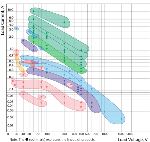
Lineup
Panasonic offers PhotoMOS for various purposes with a wide range of products.
The PhotoMOS is provided in eight types according to features and recommended purposes.
| Type name | Features | Recommended purpose |
|---|---|---|
| CC Capacitor Coupled |
Low On-resistance and low output capacitance | Measurement devices, Probe Card, Telecommunication devices, Medical devices Battery Operating Equipment |
| RF Radio Frequency |
Low On-resistance and low output capacitance | Measurement devices, Telecommunication devices, Medical devices |
| GU General Use |
Wide variation | General-purpose, amusement, and security devices, Amusement devices |
| GE General Use and Economic |
Economic and reinforced insulation | |
| HS High Sensitivity |
High Sensitivity | |
| HF High Functioned |
Low On-resistance | OA and transportation equipment, Telecommunication devices |
| HE High Functioned and Economic |
Low On-resistance, Economic | |
| Power Power |
Power, slim-shaped | Machine tools, Robots, Industrial equipment and facilities |
| PD Power DIP |
Power, flat-shaped |
 As of June 2015
Package Variations
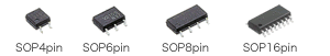
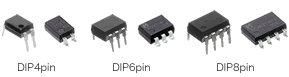
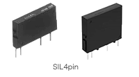
Our PhotoMOS are offered in various packages from VSSOP, the smallest-footprint in our lineup to SIL, which can control up to 10 A. We offer SOP 16 pin with 4a output and the built-in input resistor type. Panasonic has its own package options featuring their contribution to space-saving design and reducing man-hours.
PhotoMOS Package Variations
| Classification by Package Form | Classification by Implementation | |
|---|---|---|
| TSON (Thin Small Outline No lead Package) |
 |
SMD (Surface Mounted Device) |
| VSSOP (Very Shrink Small Outline Package) |
 |
|
| SON (Small Outline No lead Package) |
 |
|
| SSOP (Shrink Small Outline Package) |
 |
|
| SOP (Small Outline Package) |
 |
|
| DIP (Dual Inline Package) |
 |
SMD (Surface Mounted Device) TH (Through Hole Device) |
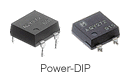
| Power-DIP (Power Dual Inline Package) |
 |
|
| SIL (Single Inline Package) |
 |
TH (Through Hole Device) |
We offer a line-up of voltage drive products with a built-in input resistor such as SSOP, SOP4pin, and SOP 16 pin. We can also meet your requirements in other packages after consultation. Please contact us.

Catalog Download
