[System Maintenance Notice]
Due to ongoing system maintenance, the site search and specification search functions are temporarily unavailable. We apologize for any inconvenience this may cause and appreciate your understanding.
【Notification of Manufacturer Change for Panasonic Industrial Devices SUNX Products and Panasonic Industrial Devices SUNX Tatsuno Products】
From April 1, 2024, the terms "Panasonic Industrial Devices SUNX Co., Ltd." and "Panasonic Industrial Devices SUNX Tatsuno Co., Ltd."
in this page and in the manuals and other documents to be downloaded will all be replaced with "Panasonic Industry Co., Ltd." and applied accordingly.
Cylindrical Inductive Proximity Sensor GX-U/GX-FU/GX-N (Discontinued Products)
We are sorry, the products have been discontinued. Please refer to the details of the discontinued products and the recommended substitutes list below.
 |
September 30, 2022 |
|
|
I/O Circuit and Wiring diagrams
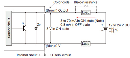
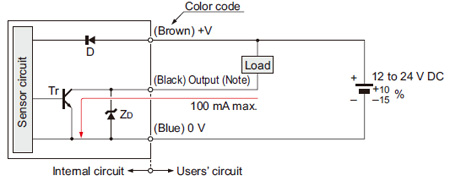
GX-□U(B)
I/O circuit diagram
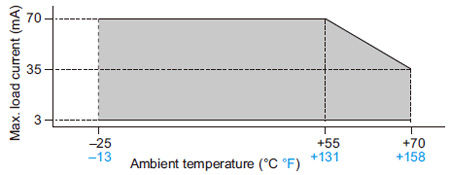
| Note: |
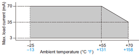
The maximum load current varies depending on the ambient temperature. |
| Symbols・・・ |
ZD: Surge absorption zener diode
Tr : PNP output transistor |
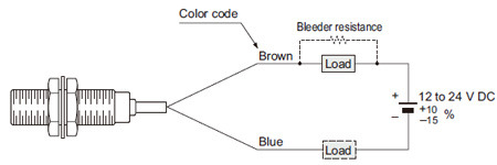
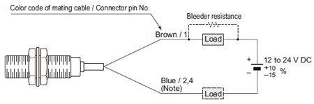
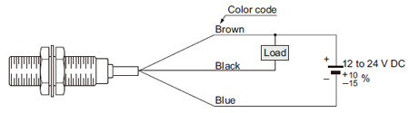
Wiring diagram
Conditions for the load
| 1) |
The load should not be actuated by the leakage current (0.8 mA) in the OFF state. |
| 2) |
The load should be actuated by (supply voltage – 3 V) in the ON state. |
| 3) |
The current in the ON state should be between 3 to 70 mA DC.
[In case the current is less than 3 mA, connect a bleeder resistance in parallel to the load so that a current of 3 mA, or more, flows.] |
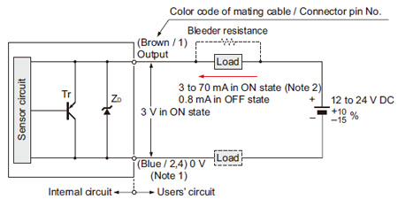
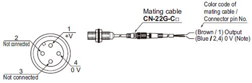
GX-□U(B)-J GX-F□U-J
| Spatter-resistant of DC 2-wire type |
I/O circuit diagram
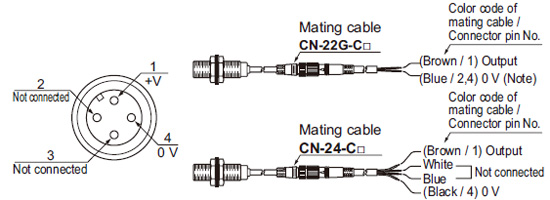
Notes:
| 1) |
This is when the mating cable CN-22G-C□ is connected. The connecter pins No.2 and No.4 are short-circuited inside the mating cable connecter. However, when the mating cable CN-24-C□ is connected;
GX-□U-J (normally open): (Black / 4) 0 V
GX-□UB-J (normally closed): (White / 2) 0 V |
| 2) |
The maximum load current varies depending on the ambient temperature. |
Conditions for the load
| 1) |
The load should not be actuated by the leakage current (0.8 mA) in the OFF state. |
| 2) |
The load should be actuated by (supply voltage – 3 V) in the ON state. |
| 3) |
The current in the ON state should be between 3 to 70 mA DC.
[In case the current is less than 3 mA, connect a bleeder resistance in parallel to the load so that a current of 3 mA, or more, flows.] |
| Symbols・・・ |
ZD: Surge absorption zener diode
Tr : PNP output transistor |
Wiring diagram
| Note: |
This is when the mating cable CN-22G-C□ is connected. The connecter pins No.2 and No.4 are short-circuited inside the mating cable connecter.
However, when the mating cable CN-24-C□ is connected;
GX-□U-J (normally open): Black / 4
GX-□UB-J (normally closed): White / 2 |
| GX-□UB-J (Normally closed) |
| GX-F□U-J (Spatter-resistant type) |
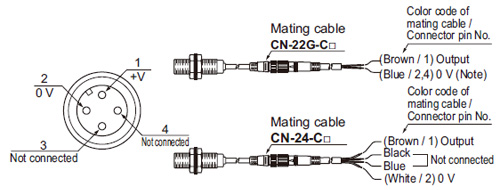
GX-N□
| DC 3-wire type (NPN output) |
I/O circuit diagram
| Note: |
If a capacitive load is directly connected to the output, malfunction may occur. |
| Symbols・・・ |
D : Reverse supply polarity protection diode
ZD: Surge absorption zener diode
Tr: NPN output transistor |
Return to top
Return to top

 Business
> Industrial Devices
> Automation Controls Top
> FA Sensors & Components
> Sensors
> Inductive Proximity Sensors
> Cylindrical Inductive Proximity Sensor GX-U/GX-FU/GX-N(Discontinued Products)
> I/O Circuit and Wiring diagrams
Business
> Industrial Devices
> Automation Controls Top
> FA Sensors & Components
> Sensors
> Inductive Proximity Sensors
> Cylindrical Inductive Proximity Sensor GX-U/GX-FU/GX-N(Discontinued Products)
> I/O Circuit and Wiring diagrams